
EUV Pellicle Market Size, Share, and Forecast 2026 to 2034
REPORT DETAILS
EUV Pellicle Market Summary
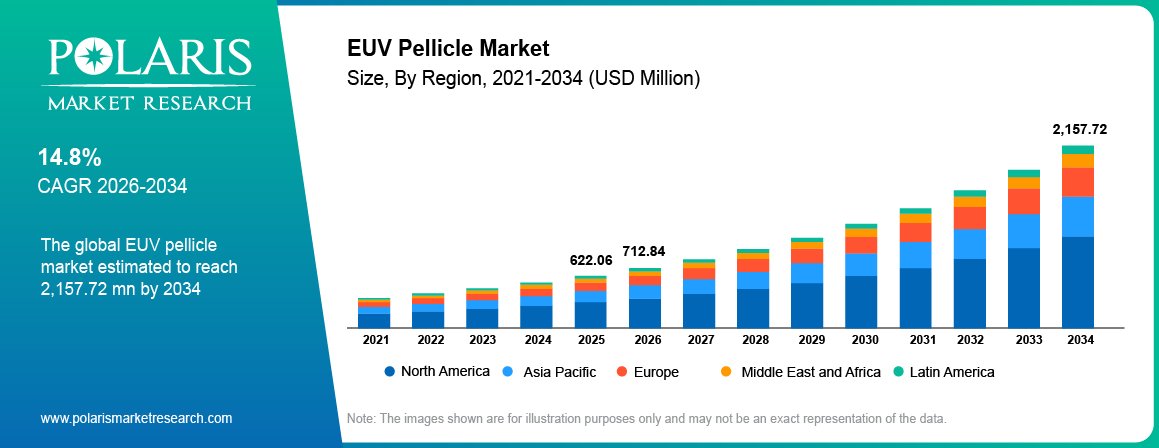
The EUV Pellicle market size was valued at USD 622.06 million in 2025. The market is expected to grow at a CAGR of 14.8% from 2026 to 2034. Growth is driven by high-NA EUV adoption, higher scanner power needs, carbon nanotube membrane development, local sourcing, and larger photomask formats.
Market Statistics
EUV Pellicle Market Key Takeaways 2025
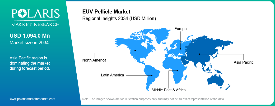
- Asia Pacific dominated the EUV pellicle industry with 63.84% in 2025, driven by EUV pellicle manufacturing and qualification programs across Japan, South Korea, and Taiwan.
- North America is expected to register 15.29% CAGR during 2026–2034, driven by High-NA EUV development and advanced semiconductor manufacturing.
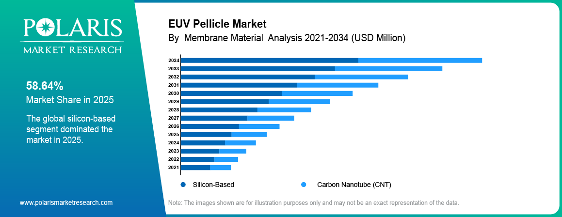
- Silicon-based membranes dominated the membrane material segment with 58.64% in 2025, due to established use in EUV production.
- Low-NA pellicles dominated the scanner power/NA compatibility segment with 82.64% in 2025, due to established 0.33 NA EUV systems.
- Foundries dominated the end-user segment with 50.86% in 2025, driven by high EUV exposure volumes.
Note: Figures and projections outlined in this report are the result of Polaris Market Research’s proprietary analytical processes, grounded in the latest available datasets and market observations
EUV Pellicle Market Definition
The extreme ultraviolet pellicle market consists of ultra-thin membranes with high transmittance fixed on special frames above EUV photomasks. These membranes protect the photomask from particulate contamination which can transfer defects to the wafers during exposure (Source: pmc.ncbi.nlm.nih.gov). The EUV photomask pellicle market includes pellicles qualified for ASML's 0.33 NA Low-NA and 0.55 NA High-NA platforms (Source: zeiss.com) Peer-reviewed research has identified important production requirements to include transmittance greater than about 88% to 90%, low membrane deflection, and long exposure durability (Source: ncbi.nlm.nih.gov)
DUV pellicles, display and touchscreen protective films, EUV mask blanks and EUV mask inspection or pellicle monitoring systems are not part of the market. DUV pellicles are made of different materials and work under different optical conditions, since the fluoropolymer membranes used for 193 nm DUV lithography absorb too strongly at the 13.5 nm EUV wavelength to be usable (Source: spiedigitallibrary.org) EUV pellicles require special membrane structures that can transmit 13.5 nm EUV radiation while offering mechanical and thermal stability (Source: ncbi.nlm.nih.gov).
Market development depends on EUV scanner deployment and the power level required by each scanner generation. Higher EUV power increases the thermal burden on the membrane, since limited transmittance causes the pellicle to absorb EUV photons and heat up during exposure (Source: pmc.ncbi.nlm.nih.gov). Therefore, manufacturers need higher transmittance and improved durability to limit throughput losses. High-NA systems introduce another engineering challenge because their exposure field is half the size of the previous generation's, and the different angle of incidence affects membrane heating and optical performance.
The September 2026 12-inch photomask initiative adds another growth variable. A larger mask requires a different pellicle format, which creates a new engineering and qualification requirement rather than a simple increase in existing pellicle production.
Market Dynamics
Driver Impact Analysis
| Market Driver | Geographic Relevance | Impact Timeline |
| 12-Inch Photomask Development | Asia Pacific (Taiwan, South Korea), North America (Intel, ASML's US operations), Europe (ASML headquarters) — the four founding members span all three regions where EUV capacity exists | Long-term: pilot line targeted for 2031, full production readiness by 2033; near-term effect is R&D and specification-setting only |
| Localization of EUV Supply Chains | Asia Pacific (South Korea, Taiwan) primarily, extending to North America via Samsung's Taylor, Texas fab | Ongoing since 2020–2021 equity stakes; near-to-medium term, with the Taylor, Texas contract already live in 2026 |
| Export Controls on EUV Pellicles | Asia Pacific (Japan as exporter; South Korea and Taiwan as the affected importers) | Immediate and ongoing since the 2024 circular amendment, with continuing effect through the forecast period |
| Carbon Nanotube Pellicle Development | Asia Pacific (Japan's Mitsui Chemicals, South Korea's FST), Europe (Finland's Canatu as equipment supplier, Belgium's imec as research partner) | Medium-term: imec–Mitsui partnership signed December 2023, production capacity committed May 2024, commercial introduction targeted 2025–2026 |
| High-NA EUV Qualification Cycle | North America (Intel's D1X facility, Oregon), Europe (ASML's scanner platform) | Near-term and accelerating: over one million cumulative High-NA wafers processed as of September 2026, with qualification activity already outpacing installed base |
Source: Polaris Market Research Analysis
Two forces are reshaping this market at once: a mask-format transition forcing every pellicle supplier to redevelop for a larger surface, and a power ceiling forcing a shift from silicon to carbon nanotube membranes. Both are detailed below.
Driver: 12-Inch Photomask Development Creates New Extreme Ultraviolet Pellicle Market Requirements
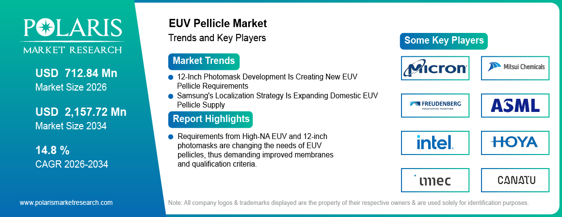
The development of 12-inch photomasks is creating new requirements for EUV pellicle dimensions, durability, frame designs, and mounting systems. Larger mask formats may need pellicles for optical transmission, mechanical stability and thermal performance over the larger area. The reduced material durability is also becoming more relevant with the hydrogen plasma exposure in advanced EUV environments. In September 2026, one of the 12-inch mask industry initiatives backed the development of the infrastructure for next-generation EUV lithography and pellicle technologies as part of the overall High-NA EUV ecosystem. The developments are raising the R&D and qualification requirements for the EUV pellicle industry, forcing suppliers to develop larger, more durable and High-NA compatible pellicle solutions (Source: eurekalert.org).
Driver: Localization of EUV Supply Chains Expands Domestic Pellicle Production
The advanced semiconductor supply chain localization is driving demand for domestic EUV pellicle manufacturing capacity. Local production can shorten procurement lead times, supply risks and dependence on overseas suppliers, and Samsung's approach to this problem illustrates how deliberate the shift has become. In 2020, Samsung took an 8 percent equity stake in S&S Tech for roughly USD 49.8 million and followed in 2021 with a 6.9 percent stake in Freudenberg Sealing Technologies, moves aimed explicitly at building a domestic alternative to Japan's Mitsui Chemicals for EUV pellicle supply (Source: digitimes.com).
That equity commitment has since matured into live commercial activity: Samsung and Freudenberg Sealing Technologies (FST) are now negotiating unit pricing, and Samsung has awarded FST a KRW 25 billion contract for pellicle handling equipment at its Taylor, Texas fab. Samsung's collaboration with S&S Tech runs deeper still, extending into shared intellectual property, with the two companies jointly filing a pellicle frame patent in March 2024 that was disclosed in late 2025, giving Samsung co-ownership of frame-level design alongside its equity position in the membrane supplier itself (Source: image-ppubs.uspto.gov). This greater localization is, therefore, creating more opportunities for suppliers that can provide qualified products and technical support close to sophisticated semiconductor manufacturing clusters.
Restraint: Export Controls Increase Cross-Border Procurement Complexity
Export controls on advanced semiconductor materials are creating procurement challenges for the EUV pellicle industry. In 2024, Japan added EUV pellicles to its controlled export regime, requiring individual licenses for some shipments. The disruption such controls can cause is not hypothetical: Japan's 2019 restriction on three other semiconductor chemical inputs to South Korea cut Japanese hydrogen fluoride exports to Korea by 96.8 percent and forced Korean buyers to reallocate sourcing to Belgium, the United States, and Taiwan within months, the clearest available precedent for how sharply this kind of control can redirect a supply chain. (Source: cepr.org). Such requirements could increase compliance costs, lengthen procurement times and present challenges for chipmakers reliant on international suppliers. These restrictions can also enhance the significance of alternative suppliers and regional production capabilities. Manufacturers may need to qualify additional sources to reduce supply-chain risks which can lead to increased testing, approval and inventory requirements. Such factors can delay procurement and complicate cross-border supply of specialized EUV pellicles.
Opportunity: Carbon Nanotube Pellicles Can Increase Power Handling
High optical transmission and power durability of carbon nanotube pellicles are needed for increasing power requirements of EUV scanners. As power levels increase, thermal loading of pellicles becomes an issue, and membranes that can hold up transmission and structural stability in harsh environments are in demand. Imec and Mitsui Chemicals are developing CNT pellicles with a target of more than 94% transmittance and power durability of over 1,000 W. Further development of CNT materials and fabrication processes will enhance their suitability for high power EUV applications. With the increased power of scanners, CNT pellicles will expand the pallet of materials available for next generation EUV lithography (Source: advancedcarbonscouncil.com).
Opportunity: High-NA EUV Creates a New Pellicle Qualification Cycle
The transition to 0.55 NA High-NA EUV systems is driving new qualification requirements for pellicle membranes, frames and mounting technologies. Demand for specialized pellicle designs is increasing as high-NA platforms have different optical and thermal requirements than 0.33 NA systems. By September 2026, High-NA EUV systems will have processed more than one million cumulative wafers – a sign of increasing equipment utilization and qualification activity. As adoption expands, suppliers developing High-NA-compatible membranes can address new qualification requirements. The transition can also encourage regional and in-house pellicle development to improve supply control and support technology qualification.
EUV Pellicle Market Segmentation Analysis
The report offers an in-depth analysis of the EUV pellicle market segmented by membrane material, scanner power/NA compatibility, end user and region to identify key revenue pockets and high-growth areas.
Membrane Material Insights
Silicon-based membranes held an 58.64% share in 2025, making them the leading membrane material in the EUV pellicle market. They are already qualified for the current Low-NA EUV production lines, and are expected to continue to be adopted by semiconductor manufacturers. Mo-Si designs provide high transmittance and power durability for current EUV applications, and established manufacturing processes and qualification history reduce the need for immediate material substitution. Silicon-based pellicles also include polysilicon and metal-silicide approaches that are evaluated on optical transmission, mechanical stability, durability and compatibility with EUV exposure conditions. As semiconductor makers are still operating with 0.33 NA systems, the current silicon-based pellicles will remain a key component for production and replacement demands.
Carbon nanotube pellicles are projected to grow at a 16.73% CAGR between 2026 and 2034, driven by rising EUV scanner power needs. CNT membranes are being developed that offer higher optical transmission and greater power durability than existing silicon-based technologies. Mitsui Chemicals’ CNT design aims for over 94% transmittance and power durability above 1,000 W. Freudenberg Sealing Technologies is working on separate CNT technology. The increased power of the scanner increases the thermal loading on pellicles and thus provides a demand for materials that can sustain the performance under more demanding exposure conditions. Therefore, continued development and qualification of CNT membranes can broaden their applicability to next generation EUV systems and create a larger opportunity for advanced pellicle materials.
Polysilicon represented 53.25% of the EUV pellicle material market share in 2025. The material is evaluated for its suitability for EUV exposure conditions, including membrane performance, optical characteristics, mechanical properties, and compatibility with manufacturing processes. The demand is based on the capability of polysilicon membranes to provide enough transmission and robustness with dimensional stability under exposure. The segment is still part of the larger silicon-based pellicle category and is subject to the continued operation of established EUV production platforms. As scanner power increases, manufacturers will look at other materials for more demanding EUV applications, and qualification requirements across semiconductor manufacturing environments will determine how long polysilicon remains relevant.
In 2025, Mo-Si membranes represented 31.25% of the silicon-based EUV pellicle market. Mo-Si is an established approach used in commercial EUV pellicle designs and is still relevant to current Low-NA production requirements. The qualification today and proven performance of proven Mo-Si solutions give semiconductor manufacturers increased confidence. Mitsui Chemicals’ Mo-Si design exhibits high transmittance and about 400 W power durability for EUV applications. However, increasing scanner power can raise thermal demands on the membrane, requiring continued evaluation of transmittance, durability, and exposure performance. The segment will therefore remain connected to the installed Low-NA EUV base while suppliers develop alternative materials for higher-power and High-NA applications.
Metal-silicide membranes represented an 15.5% share in 2025 within the silicon-based EUV pellicle material category. The technology is evaluated in terms of EUV transmittance, membrane durability, mechanical stability, and hydrogen plasma durability. Increasingly demanding EUV environments are placing a greater emphasis on the durability of the membranes, while maintaining adequate optical performance. Qualification requirements remain important because pellicles must perform reliably under semiconductor manufacturing conditions without imposing unacceptable throughput or defect risks. Ongoing development of metal-silicide materials can thus aid the industry’s quest for better membrane performance. The commercial adoption will depend on the ability of these materials to provide the required combination of optical transmission, mechanical properties, exposure lifetime, and compatibility with manufacturing.
Scanner Power / NA Compatibility Insights
Low-NA, 0.33 NA compatible pellicles held an 82.64% share in 2025, making them the established compatibility segment in the EUV pellicle market. Existing EUV production lines still use qualified pellicles designed for 0.33 NA scanner platforms and proven EUV scanner power level requirements. This installed equipment base creates a recurring demand for qualified pellicles, replacements and associated maintenance activities. Manufacturers also benefit from existing qualification and production experience, reducing the immediate need to switch to new membrane technologies. While High-NA systems are opening new opportunities, the ongoing operation of Low-NA EUV systems will sustain demand for proven pellicle designs during the forecast period.
High-NA, 0.55 NA compatible pellicles are expected to record a 16.48% CAGR over 2026 to 2034 due to growing deployment and qualification of ASML’s High-NA EUV systems. The change in the numerical aperture affects the exposure conditions and introduces new optical and thermal requirements for pellicles. Therefore, suppliers will need to develop membranes and frames that can maintain transmission, durability and mechanical stability at High-NA conditions. The current RD source material indicated that more than 1 million cumulative wafers were processed on High-NA EUV systems by September 2026. Increased use of high NA can translate into more qualification work and opportunities for specialized pellicle suppliers.
End User Insights
Foundries held 50.86% of the EUV pellicle market share in 2025, with the end-user segment dominating the market. Foundries run high-end semiconductor manufacturing facilities where EUV exposure volumes repeatedly generate needs for qualified pellicles, replacement products, maintenance and security of supply. As EUV production ramps, the need for reliable pellicle availability is increasing, as membrane performance can affect mask protection and manufacturing continuity. Foundries are also looking at alternative sourcing strategies, including relationships with domestic suppliers and in-house production. These approaches may increase demand for qualification, inspection and process-control capabilities and create opportunities for suppliers that can meet stringent technical and supply requirements.
Integrated device manufacturers accounted for 36.72% share in 2025, supported by increasing EUV deployment across leading-edge semiconductor production. IDMs should evaluate membrane performance against optical, thermal, and exposure requirements and select pellicles that are compatible with current and developing scanner platforms. With the evolution of High-NA EUV, as newer systems introduce different operating conditions, there is a growing demand for dedicated pellicle designs. Intel’s High-NA EUV activities are assisting in qualification requirements for next generation pellicle technologies. As IDMs become more advanced in semiconductor manufacturing, there may be a growing demand for qualified third-party suppliers, advanced membrane materials and technologies with adequate transmittance, durability and supply reliability.
Mask shops had a 12.42% share in 2025, due to their involvement in photomask preparation, pellicle mounting, and qualification activities. Mask dimensions, mounting systems, inspection requirements and exposure conditions must be considered together in the evaluation of pellicle compatibility. The development of larger photomask formats is creating additional requirements for pellicle dimensions and frame engineering. Mask shops therefore form an important link between pellicle suppliers, mask manufacturers, and semiconductor manufacturers during qualification. As the industry prepares for future High-NA systems and 12-inch photomasks, mask shops can become increasingly involved in validating new pellicle formats, mounting approaches, and compatibility requirements before commercial production deployment.
Regional Analysis
Asia Pacific EUV Pellicle Market Trends
Asia Pacific led the EUV pellicle market in 2025 with a share of approximately 63.84%, owing to the concentrated semiconductor manufacturing and supplier development in Japan, South Korea, and Taiwan. Japan continues to be a major source of supply through Mitsui Chemicals, South Korea is developing domestic suppliers through Samsung’s relationships with S&S Tech and Freudenberg Sealing Technologies (FST), and TSMC is going in-house in Taiwan. In February 2026, LINTEC developed a dual-density CNT pellicle with improved durability at 300-400°C to address EUV pellicle performance challenges as source power increases. With the increase of Low-NA production and progress in High-NA qualification, the region is expected to retain its dominant position (Source: lintec-global.com).
North America EUV Pellicle Market Trends
North America is expected to register a 15.29% CAGR from 2026 to 2034, supported by High-NA EUV development and expansion of advanced semiconductor manufacturing in the US. Intel and Samsung are contributing to regional EUV deployment and pellicle-related activities. Intel Foundry processed over a million cumulative wafers with High-NA EUV systems by September 2026 raising the requirements for next-generation pellicles and related mask technologies. The growth of advanced semiconductor manufacturing capacity can generate regional demand for qualified pellicles, technical support and supply chain capabilities. Suppliers who can meet new optical, thermal, and durability requirements have opportunities in the development of High-NA infrastructure (Source: intel.com).
Europe EUV Pellicle Market Trends
In 2025, Europe accounted for 17.42% of the EUV pellicle market share, due to EUV scanner development, semiconductor research and advanced manufacturing activities. ASML and imec contribute to the development of the regional EUV technology ecosystem through equipment development, research and industry collaboration. The European Semiconductor Manufacturing Company fab in Germany aims to produce 480,000 300mm wafers annually by 2029 to meet future demand for EUV-related technologies. The region also remains important for pellicle qualification because EUV scanner development and semiconductor research activities require close coordination among equipment manufacturers, research institutions, mask suppliers, and semiconductor manufacturers. These activities support continued regional demand for advanced pellicle technologies (Source: ec.europa.eu).
Latin America EUV Pellicle Market Trends
Latin America accounted for an 2.61% share of the EUV pellicle market in 2025, while regional demand remained limited compared with major EUV manufacturing centers. The region does not currently have the same concentration of disclosed advanced EUV semiconductor manufacturing and pellicle production programs as Asia Pacific, North America, or Europe. So demand is mostly tied to the wider semiconductor supply chains and any future potential investments in manufacturing. As regional production capabilities grow, an accumulation of advanced semiconductor infrastructure may create additional demand for EUV-related technologies. Future adoption of EUV pellicles in the region will be contingent on the development of supporting technical infrastructure, supplier networks and semiconductor manufacturing capacity.
Middle East & Africa EUV Pellicle Market Trends
The Middle East & Africa held a 3.77% share in the EUV pellicle market in 2025, reflecting the region's developing position in advanced semiconductor manufacturing and associated infrastructure. In the EU, the production and qualification activity for EUV pellicles is currently limited when compared to established semiconductor manufacturing centers. Future regional demand will be driven by investment in advanced semiconductor plants, technology infrastructure and supporting supply chains. Growth in semiconductor-related investment could create opportunities for EUV technology suppliers and technical service providers if advanced lithography capabilities are established. Development of local technical expertise and partnerships with international semiconductor companies will also influence future adoption.
Regulatory Heatmap Analysis
| Region/Country | Regulation | Status | Impact on EUV Pellicle Market |
| Japan | METI controlled export list, pellicle-specific amendment | In effect since 2024; individual export licenses required for shipments outside white-listed destinations | Direct and severe: Mitsui Chemicals, the market's largest supplier, must now obtain individual licenses for pellicle shipments, adding compliance and lead-time cost to the Japan-to-Taiwan and Japan-to-Korea trade lanes this market has historically run on |
| Netherlands | Dutch government export license requirement on ASML DUV and EUV lithography systems | Expanded September 2024 to cover more DUV models; EUV systems already under license requirement since 2019 | Indirect but significant: controls the scanner platform pellicles are qualified against, not pellicles themselves, but any restriction on where ASML can ship EUV scanners caps where pellicle demand can develop in the first place |
| European Union | EU Control List incorporation of Dutch national controls | In effect since November 2025; extends the Dutch license requirement to all EU member states | Indirect: formalizes what was previously a Netherlands-only rule across the EU, reinforcing Europe's role in this market as scanner-design and specification-setting rather than pellicle manufacturing |
| South Korea and Taiwan | Wassenaar Arrangement membership | Bulk-license carve-out applies to both, as Wassenaar members | Softens the practical impact of Japan's 2024 pellicle listing for this market's second- and third-largest buyer bases, but does not eliminate it, since each shipment still requires license application and end-user documentation the pre-2024 process did not demand |
| United States | US Export Administration Regulations, aligned with Dutch and Japanese controls since September 2024 | In effect; primarily targets chip manufacturing equipment and technology destined for China | Indirect for this market specifically: no disclosed restriction on Intel's own Mitsui-sourced pellicle supply, but reinforces the broader trend of allied governments treating EUV supply chain components as strategic materials, the same framing driving Japan's pellicle-specific listing |
Source: ASML Holding N.V. Annual Report (SEC Form 6-K), Baker McKenzie Sanctions & Export Controls Blog, company disclosures and Polaris Market Research Analysis
EUV Pellicle Market Competitive Landscape
The EUV pellicle market remains concentrated among a limited group of qualified or qualifying suppliers. Mitsui Chemicals represents the established Japanese supplier base, while S&S Tech and Freudenberg Sealing Technologies (FST) are developing South Korea's domestic supply capabilities. TSMC represents an in-house production model, adding a vertically integrated approach to the competitive landscape and reducing dependence on external pellicle suppliers.
ASML occupies a distinct position as the EUV scanner OEM and an early developer of EUV pellicle technology. The company's scanner specifications influence the technical requirements for commercial pellicle suppliers. High-NA EUV development is also creating new requirements related to membrane performance, power durability, transmittance, and compatibility, shaping technology development across the supplier landscape.
EUV Pellicle Competitive Landscape Snapshot
| Company | Estimated Market Position | Competitive Anchor | Notable 2024–2026 Move |
| Mitsui Chemicals, Inc. | Market Leader | Incumbent Low-NA supplier, CNT pipeline | Committed CNT production capacity, May 2024 |
| ASML Holding N.V. | Established — Scanner OEM | Scanner OEM and original pellicle developer | EXE:5200B sets the High-NA design standard |
| S&S Tech Co., Ltd. | Emerging Challenger | Korean domestic MeSi/CNT supplier | Co-filed pellicle frame patent with Samsung |
| Freudenberg Sealing Technologies (FST) | Emerging Challenger | Korean CNT supplier, Canatu-sourced synthesis | Won KRW 25B Samsung Taylor, TX contract |
| Taiwan Semiconductor Manufacturing Company | Established — Vertically Integrated | In-house production, not an open-market supplier | Converting Fab 3 to in-house pellicle production |
| Samsung Electronics | Anchor Buyer — Localization Driver | Foundry and equity-backed sourcing strategy | Holds equity stakes in S&S Tech and FST |
| Intel Corporation | Anchor Buyer — External Supplier Reliant | IDM, scanner OEM alignment | Passed 1M wafers on High-NA EUV at D1X |
| SK Hynix | Anchor Buyer — Emerging Demand | Memory manufacturer expanding EUV use | No disclosed localization program |
| Micron Technology | Anchor Buyer — Emerging Demand | Memory manufacturer expanding EUV use | No disclosed localization program |
| Hoya Corporation | Established — Adjacent Supply Chain | Mask blank supplier | Named in Samsung's localization push |
| Toppan Photomasks, Inc. | Established — Adjacent Supply Chain | Photomask supplier, complementary role | Showcased added capacity at SEMICON Japan 2025 |
| imec | Upstream — Research and Licensing | CNT membrane research and licensing | Signed CNT partnership with Mitsui, Dec 2023 |
| Canatu | Upstream — Equipment Supplier | CNT synthesis equipment supplier | Supplies FST's CNT reactor equipment |
Source: Company filings, regulatory disclosures and Polaris Market Research Analysis
Competitive positioning increasingly depends on pellicle qualification, buyer relationships, power durability, transmittance, frame engineering, and supply security. Suppliers are developing different strategies around established Low-NA products, CNT technologies, domestic production, and in-house manufacturing. These approaches are creating distinct competitive positions across Japan, South Korea, Taiwan, and the broader EUV semiconductor supply chain.
EUV Pellicle Market Technology and Innovation Landscape
Technology and Innovation Landscape Snapshot
| Technology | Leading Developer(s) | Key Specification | Status |
| Carbon Nanotube (CNT) Membranes | imec, Mitsui Chemicals | Above 94% transmittance, beyond 1,000W durability | Commercial introduction targeted 2025–2026 |
| CNT Membranes (independent route) | Freudenberg Sealing Technologies, Canatu | Hydrogen-plasma-resistant coating on CNT membrane | In qualification, unit pricing under negotiation |
| Mo/Si Silicon-Based Membranes | Mitsui Chemicals | Over 90% transmittance, 400W power durability | Current commercial standard for Low-NA |
| Pellicle Frame Engineering | Samsung Electronics, S&S Tech | Titanium-alloy frame, patent-protected design | Jointly patented, disclosed late 2025 |
| Actinic Mask Inspection | Lasertec | Inspects masks at the 13.5nm EUV exposure wavelength itself | Sole commercial supplier; adoption gates pellicle qualification |
| High-NA Pellicle Qualification | ASML, Mitsui, Intel | Designed for EXE:5200B's narrower field and steeper angle of incidence | No High-NA-specific pellicle has shipped commercially as of this report |
Source: Company filings and and Polaris Market Research Analysis
Carbon nanotube membranes represent a major material innovation in the EUV lithography pellicle market. Imec and Mitsui Chemicals entered a commercialization partnership, followed by Mitsui's production capacity commitment. CNT development focuses on improving membrane performance for higher-power EUV applications and creating an alternative to established silicon-based pellicle technologies.
Pellicle frame engineering represents another area of technology development. Samsung and S&S Tech had intellectual property on specialized pellicle frame designs. During EUV exposure, the frame materials need to provide thermal stability, mechanical strength and dimensional accuracy. These requirements add to the engineering considerations for suppliers developing pellicles for advanced lithography applications.
Actinic mask inspection also connects closely with EUV pellicle qualification. EUV masks require inspection methods that identify defects under relevant EUV wavelengths. The source material identifies Lasertec as a concentrated supplier of commercial actinic mask inspection equipment. Inspection capabilities therefore form an important part of the broader EUV mask and pellicle technology ecosystem.
These developments create a connected technology chain covering the pellicle membrane, frame, photomask, inspection equipment, and EUV scanner. Improvements across these components influence pellicle qualification requirements and technology development. Suppliers therefore need to consider membrane performance, frame design, mask compatibility, inspection requirements, and scanner conditions when developing next-generation EUV pellicle solutions.
Use Case Analysis
Foundry In-House Production
TSMC's Fab 3 conversion illustrates the in-house EUV pellicle production model. The goal is to better control cost, supply timing and repair activities. The model decreases dependency on external suppliers but requires investment in internal manufacturing, qualification, inspection and process control.
IDM High-NA Qualification
Intel's D1X facility offers a High-NA qualification use case. By September 2026, Intel and ASML reported that more than one million cumulative wafers were processed on High-NA EUV tools. High-NA pellicle selection is important because the technology introduces different optical and thermal conditions from Low-NA exposure.
Foundry Domestic Localization
Samsung's Taylor facility demonstrates how domestic supplier development can extend across international manufacturing locations. Samsung awarded Freudenberg Sealing Technologies (FST) a USD 18.03 million contract for EUV pellicle handling equipment at the Texas site. The use case links Korean pellicle development with US semiconductor manufacturing expansion.
Large Mask Consortium Format Transition
The Large Mask Consortium represents a future use case centered on 12-inch photomasks to address reticle stitching challenges. This shift requires the co-evolution of mask blanks, pellicles, writing tools, inspection, and manufacturing. The consortium targets a 2031 pilot line, creating a multi-year development period for the EUV pellicle industry.
Buyer Analysis and Barriers to Market Entry
Buyer Decision Framework
| Buyer Type | Primary Decision Driver | Representative Example |
| Foundries (TSMC, Samsung Foundry) | Supply security, in-house or equity-backed sourcing | TSMC Fab 3 conversion; Samsung's S&S Tech and Freudenberg Sealing Technologies (FST) equity stakes |
| Integrated Device Manufacturers (Intel) | External supplier qualification, scanner OEM alignment | Reliance on ASML/Mitsui-qualified pellicles for High-NA D1X deployment |
| Mask Shops / Consortium Programs | Format standardization, multi-year roadmap alignment | Large Mask Consortium 12-inch photomask and pellicle redevelopment commitment |
EUV pellicle purchasing depends on qualification risk rather than price alone. Buyers evaluate membrane transmittance, power durability, defect rates, mechanical performance, supplier capacity, delivery reliability and qualification history.
Barriers to Market Entry
- Qualification criteria: New vendors must provide extensive documentation, batch testing, process qualification, and customer qualification.
- Performance criteria: The membranes should have high transparency, low deflection, thermal stability, and adequate exposure lifetime.
- Capital criteria: The manufacturing process will involve specialized membrane production and a controlled environment.
- Risk of changing customers: There are high risks for the semiconductor manufacturer in case of production difficulties with a new pellicle.
- Export controls: Overseas vendors may be subject to additional licensing restrictions.
- High-NA requirements: New scanner generations require additional optical and thermal qualification.
- Future 12-inch format: New entrants need to decide whether to focus on the current 6-inch format or future larger-mask requirements.
EUV Pellicle Market Premium Insights and Forward Outlook
12-Inch Photomasks Could Trigger a New Qualification Cycle
The 12-inch photomask initiative represents a significant future engineering requirement. The consortium's 2031 pilot-line target provides suppliers with several years to develop new membrane and frame specifications. Suppliers that participate early in specification development could influence future qualification standards. The opportunity depends on successful technical development and customer acceptance.
Supplier Localization Is Reshaping the Competitive Structure
Samsung, TSMC, and Intel represent three different sourcing strategies. Samsung is developing domestic supplier relationships. TSMC is pursuing in-house production. Intel continues to rely on external qualified suppliers. This divergence means supplier opportunities differ by customer. A supplier strategy suitable for Samsung may not apply to TSMC or Intel.
Carbon Nanotube Technology Could Change Supplier Economics
CNT pellicles target higher transmittance and substantially higher power durability than established silicon-based designs. Commercial success depends on whether manufacturers can maintain these performance levels at a production scale while controlling defect rates and cost.
Cost and Pricing Benchmarking Analysis
EUV pellicles operate at a substantially higher price point than DUV pellicles. Publicly disclosed pricing also indicates variation between established products and newer products under qualification. The available price points should not be treated as directly comparable commercial quotations. The Freudenberg Sealing Technologies (FST) figure relates to an early-stage negotiation, while the ASML figure represents an earlier pricing precedent.
Key Players in the EUV Pellicles Market
- ASML Holding N.V.
- Canatu
- Freudenberg Sealing Technologies (FST)
- Hoya Corporation
- Imec
- Intel Corporation
- Micron Technology
- Mitsui Chemicals, Inc.
- Samsung Electronics
- S&S Tech Co., Ltd.
- SK Hynix
- Taiwan Semiconductor Manufacturing Company
- Toppan Photomasks, Inc.
Industry Developments
- September 2026: TSMC, Samsung, Intel, and ASML formed the Large Mask Consortium and committed to developing a 12-inch photomask format with a 2031 pilot-line target. (Source: asml.com)
- September 2026: Intel and ASML reported more than one million cumulative wafers processed on High-NA EUV systems. (Source: finance.yahoo.com)
- January 2026: Freudenberg Sealing Technologies (FST) and Samsung discussed EUV pellicle pricing below USD 36,000. Samsung also awarded Freudenberg Sealing Technologies (FST) a USD 18.04 million Taylor, Texas contract for pellicle handling equipment. (Source: trendforce.com)
- September 2025: TSMC began converting its 8-inch Fab 3 toward in-house EUV pellicle production. (Source: techpowerup.com)
- May 2024: Mitsui Chemicals committed production capacity for CNT pellicles at Iwakuni-Ohtake Works. (Source: mitsuichemicals.com)
EUV Pellicle Market Report Segmentation
By Membrane Material Outlook (Revenue, USD Million, 2021–2034)
- Silicon-Based
- Polysilicon
- Mo-Si
- Metal-Silicide
- Carbon Nanotube (CNT)
By Scanner Power / NA Compatibility Outlook (Revenue, USD Million, 2021–2034)
- Low-NA, 0.33 NA Compatible
- High-NA, 0.55 NA Compatible
By End User Outlook (Revenue, USD Million, 2021–2034)
- Foundries
- Integrated Device Manufacturers
- Mask Shops
By Regional Outlook (Revenue, USD Million, 2021–2034)
- North America
- US
- Canada
- Europe
- Germany
- France
- UK
- Italy
- Spain
- Netherlands
- Rest of Europe
- Asia Pacific
- China
- Japan
- India
- South Korea
- Taiwan
- Australia
- Rest of Asia Pacific
- Latin America
- Brazil
- Mexico
- Argentina
- Rest of Latin America
- Middle East & Africa
- Saudi Arabia
- UAE
- South Africa
- Rest of Middle East & Africa
EUV Pellicle Market Report Scope
| Report Attributes | Details |
| Market Size in 2025 | USD 622.06 Million |
| Market Size in 2026 | USD 712.84 Million |
| Revenue Forecast by 2034 | USD 2,157.72 Million |
| CAGR | 14.8% from 2026–2034 |
| Base Year | 2025 |
| Historical Data | 2021–2024 |
| Forecast Period | 2026–2034 |
| Quantitative Units | Revenue in USD Million and CAGR |
| Report Coverage | Revenue Forecast, Growth Factors, Competitive Landscape, Industry Trends, and Strategic Analysis |
| Segments Covered |
|
| Regional Scope | North America, Europe, Asia Pacific, Latin America, Middle East & Africa |
| Competitive Landscape | Company Profiling, Product Benchmarking, Financial Analysis, Market Developments, and Strategic Initiatives |
| Report Format | PDF + Excel |
| Customization | Available by Country, Region, and Segment |
Source: Polaris Market Research Analysis
Why Choose Polaris Market Research
Polaris Market Research & Consulting, Inc. combines regulatory research, company disclosures, patent information, peer-reviewed materials research, and industry developments to assess the EUV pellicle industry.
The EUV pellicle market analysis places specific attention on scanner power and NA compatibility because the distinction separates established Low-NA products from the emerging High-NA opportunity. The analysis also examines supplier localization, in-house production, CNT technology, export controls, pricing, and the planned 12-inch photomask transition. Clients evaluating supplier relationships, regional opportunities, High-NA technology, or the future 12-inch photomask ecosystem can request a tailored scope review of the analysis.
EUV Pellicle Market Research Methodology
The EUV pellicle market report uses secondary research across regulatory publications, company announcements, patent filings, peer-reviewed materials research, semiconductor industry publications, and regional trade sources. The EUV pellicle industry forecast is based on analysis of industry developments, technology trends, supplier activities, and market dynamics. The EUV pellicle market size remains reserved for confirmed Polaris proprietary data. No third-party syndicated market-sizing figures are used as substitutes for internal estimates.
Research Methodology Phases
| Phase | Approach |
| Scope Definition | Define EUV pellicle revenue boundaries, materials, scanner compatibility, end users, and regions |
| Secondary Research | Review regulatory filings, company releases, patents, peer-reviewed studies, and semiconductor industry sources |
| Primary Research | Analyst interviews with suppliers, semiconductor manufacturers, equipment companies, and industry specialists where applicable |
| Market Modeling | Apply Polaris market sizing, segment allocation, regional analysis, and forecast methodology |
| Data Validation | Cross-check company disclosures, regulatory developments, technical specifications, pricing information, and market assumptions |
| Review and QC | Senior analyst review, source verification, consistency checks, and editorial quality control |
Source: Polaris Market Research Analysis.
The methodology distinguishes publicly disclosed technical and commercial information from Polaris proprietary market estimates. The source material identifies Japan METI filings, company disclosures, patent filings, peer-reviewed research, and Korea- and Taiwan-focused semiconductor trade sources as key inputs.
EUV Pellicle Market FAQ's
The EUV pellicle market was valued at USD 622.06 million in 2025. Japan's 2024 decision to add EUV pellicles to its controlled export list confirms the product has reached strategic-materials status regardless of its exact dollar size.
An EUV pellicle is an ultra-thin, high-transmittance membrane mounted on a frame a few millimeters above an EUV photomask to keep particles out of the focal plane during lithography exposure. Peer-reviewed research sets the working specification at above 88 to 90 percent transmittance and a lifetime beyond 315 hours under load.
The market is expected to grow at a CAGR of 14.8% from 2026 to 2034, driven by the High-NA EUV transition and the 12-inch photomask initiative TSMC, Samsung, Intel, and ASML launched on September 8, 2026.
EUV photomasks cost far more than the pellicle protecting them, and particle contamination on an unprotected mask prints directly as a chip defect. Chipmakers accept the pellicle's small transmittance loss specifically to avoid that mask damage and the yield loss it would cause.
Asia Pacific leads, hosting every disclosed production and qualification program in this report, from Japan's Mitsui Chemicals to South Korea's S&S Tech and Freudenberg Sealing Technologies to Taiwan's TSMC.
DUV pellicles use fluoropolymer membranes that absorb too strongly at EUV's 13.5 nanometer wavelength to be usable there, so EUV pellicles require entirely different materials, silicon-based or carbon nanotube membranes only 30 to 50 nanometers thick, costing roughly 20 to 50 times more per unit.
Silicon-based Mo/Si membranes lead by installed volume, demonstrated at over 90 percent transmittance and 400W power durability. Carbon nanotube membranes are the fastest-advancing category, with Mitsui Chemicals' imec-licensed design rated above 94 percent transmittance and beyond 1,000W durability.
Disclosed negotiated pricing places EUV pellicles around 20 to 50 million won, roughly USD 15,000 to USD 36,000, compared with about 1 million won for a DUV pellicle, a gap of more than 20 times.
TSMC began converting its 8-inch Fab 3 to in-house EUV pellicle production in September 2025, specifically to cut cost and lead time and integrate pellicle repair, rather than remain fully dependent on external suppliers.
High-NA EUV raises the scanner's numerical aperture from 0.33 to 0.55, sharpening resolution but roughly halving the exposable field. That narrower field forces reticle stitching for large dies, a constraint the industry's 2031 12-inch photomask pilot line is designed to remove.
Samsung took an 8 percent equity stake in S&S Tech in 2020 and a 6.9 percent stake in Freudenberg Sealing Technologies in 2021, explicitly to build a domestic alternative to Japan's Mitsui Chemicals and reduce its dependence on a single overseas supplier.
Japan added EUV pellicles to its controlled export list in 2024, requiring individual licenses for shipments outside white-listed destinations. The precedent for how disruptive this can be is not hypothetical: a similar 2019 Japanese restriction cut hydrogen fluoride exports to South Korea by 96.8 percent within months.
This report covers 2026 to 2034, with 2025 used as the base year for confirmed figures.
Download Sample Report of EUV Pellicle Market
Please fill out the form to request a customized copy of the research report.


