
Semiconductor Defect Inspection Equipment Market Trends, Industry Share, 2025-2034
REPORT DETAILS
REPORT DETAILS
ABOUT THIS REPORT
Market Statistics
Overview
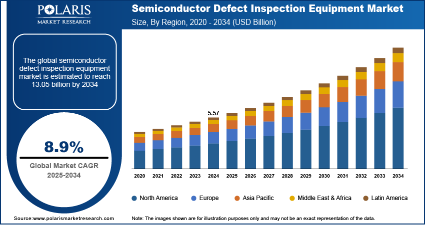
The global semiconductor defect inspection equipment market size was valued at USD 5.57 billion in 2024, growing at a CAGR of 8.9% from 2025 to 2034. Increased adoption of AI, 5G, and HPC technologies is fueling the production of complex chips, driving demand for defect inspection systems that can ensure tight process control.
Key Insights
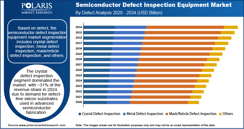
- The crystal defect inspection segment dominated the market in 2024 with ~31% of the revenue share due to demand for defect-free silicon substrates used in advanced semiconductor fabrication.
- The optical inspection segment held ~35% of the revenue share in 2024 due to its widespread adoption across multiple stages of wafer processing.
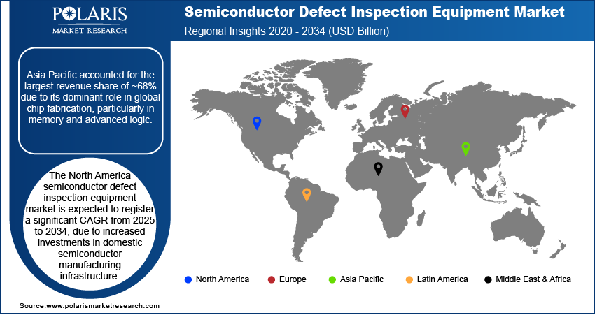
- The North America semiconductor defect inspection equipment market is expected to register a significant CAGR from 2025 to 2034 due to increased investments in domestic semiconductor manufacturing infrastructure.
- The U.S. dominated the North America market due to the rapid acceleration of fab construction and modernization projects, particularly driven by the CHIPS and Science Act.
- Asia Pacific accounted for the largest revenue share of ~68% due to its dominant role in global chip fabrication, particularly in memory and advanced logic.
- China led the Asia Pacific market due to aggressive investments in its domestic semiconductor ecosystem, aimed at reducing foreign dependency.
Industry Dynamics
- Growing demand for advanced semiconductor nodes in AI, electric vehicles, and 5G drives the need for high-precision defect inspection equipment.
- The increasing complexity of chip manufacturing processes requires more frequent and accurate inspection to ensure yield and reliability.
- Integration of AI and machine learning into inspection systems enables real-time defect detection and predictive analytics for improved efficiency.
- High capital investments and technical complexity limit adoption in small and mid-sized fabs, especially in emerging economies.
Market Statistics
- 2024 Market Size: USD 5.57 billion
- 2034 Projected Market Size: USD 13.05 billion
- CAGR (2025–2034): 8.9%
- Asia Pacific: Largest market in 2024
To Understand More About this Research: Download Sample Report
The semiconductor defect inspection equipment market focuses on tools and systems used to detect, classify, and analyze defects in semiconductor wafers, photomasks, and packaging. These systems ensure yield optimization, process control, and quality assurance during semiconductor manufacturing, supporting both front-end and back-end production. Rising global semiconductor demand is leading to the construction and expansion of fabs, particularly for leading-edge nodes. Each facility requires high-throughput, accurate defect inspection equipment to monitor wafer quality across production stages and ensure cost-effective manufacturing.
Sub-5nm transistor manufacturing increases sensitivity to nanoscale defects, demanding advanced inspection tools that identify minute pattern distortions, line-edge roughness, or particle contamination to ensure process control, high yield, and consistent chip performance. Moreover, wider adoption of 2.5D and 3D IC packaging introduces dense interconnect layers and through-silicon vias, necessitating precise defect inspection systems to detect bonding issues, delamination, or voids that compromise electrical integrity and reduce final yield.
Drivers & Opportunities
Increasing Semiconductor Fab Investments: Rising investments in semiconductor fabrication plants are playing a crucial role in driving demand for advanced semiconductor defect inspection equipment. In April 2025, TSMC announced to increase its investments in advanced semiconductor manufacturing in the U.S. by an additional USD 100 billion, building on its existing USD 65 billion investment in Arizona. This brings TSMC's total U.S. investment to ~USD 165 billion. Global chip shortages and the need for technological independence are prompting governments and private players to invest heavily in both new and existing fabs. These facilities require robust inspection systems that detect defects across multiple process nodes and stages of production. Defect inspection equipment ensures high wafer yield by identifying contaminants, micro-pattern errors, and lithography issues early in the process. The push for faster chip development cycles and reduced manufacturing costs further increases the need for efficient inspection solutions in high-volume production environments.
Rising Adoption of Semiconductors in EVs: The growing use of semiconductors in electric vehicles, driver-assistance systems, and automotive safety platforms has propelled the importance of quality control in chip manufacturing. The U.S. International Trade Commission highlights that conventional vehicles typically incorporate an average semiconductor value of USD 330, whereas hybrid electric vehicles contain semiconductor components worth between USD 1,000 and USD 3,500. Automotive applications demand extremely high levels of reliability due to the critical nature of electronic components in ensuring vehicle safety and performance. Regulatory standards such as AEC-Q100 impose rigorous inspection benchmarks to minimize the risk of failure in harsh operational conditions. Defect inspection equipment supports this need by enabling early identification of defects in power devices, microcontrollers, and sensors. Its role in maintaining compliance, improving reliability, and reducing warranty claims is becoming more critical as automotive semiconductor content continues to rise.
Segmental Insights
Defect Analysis
Based on defect, the segmentation includes crystal defect inspection, metal defect inspection, mask/reticle defect inspection, and others. The crystal defect inspection segment dominated the market with ~31% of the revenue share in 2024, due to demand for defect-free silicon substrates used in advanced semiconductor fabrication. Crystal defects, including dislocations and stacking faults, compromise structural integrity and electrical performance. Manufacturers rely on specialized inspection tools to identify such flaws early in wafer processing. Advanced lithography and sub-10nm geometries heighten the sensitivity to minor substrate imperfections, making crystal inspection vital to yield management. Foundries are expanding their capabilities in high-volume production, creating further reliance on equipment that ensures consistent substrate quality across thousands of wafers.
The metal defect inspection segment is expected to register the highest CAGR from 2025 to 2034, driven by increasing transistor density and multi-layer interconnect complexity in advanced chip designs. Detecting metal voids, residues, and bridging faults is essential in maintaining conductivity and performance across shrinking nodes. As chipmakers adopt EUV lithography and implement more metal layers in BEOL processes, inspection accuracy becomes more critical. Metal defect inspection tools are evolving to offer higher resolution and depth sensitivity, allowing real-time detection of buried defects in copper and cobalt interconnects. This advancement supports both production yield goals and reliability requirements in performance-driven applications such as AI accelerators and high-speed memory.
Technology Analysis
In terms of technology, the segmentation includes, optical inspection, electron beam inspection, x-ray inspection, and others. The optical inspection segment held ~35% of the revenue share in 2024 due to its widespread adoption across multiple stages of wafer processing. The technology offers high-throughput and cost-effective solutions for surface-level defect detection on patterned and unpatterned wafers. Optical tools are optimized for inline monitoring, enabling quick feedback loops during mass production. Improvements in resolution, lighting techniques, and image processing allow the detection of smaller defects without slowing production speed. Optical inspection remains a first-line method in quality control strategies, particularly valuable in logic and memory fabs requiring continuous yield optimization.
The electron beam inspection segment is expected to grow significantly from 2025 to 2034 due to its ability to detect ultra-fine defects below the resolution limits of optical systems. Shrinking process nodes and the introduction of high-aspect-ratio features demand inspection tools that offer nanometer-level sensitivity. E-beam systems are especially suited for analyzing contact holes, vias, and metal lines in advanced 3D architectures. Adoption is growing among leading-edge fabs that produce high-performance chips for AI, HPC, and automotive applications. While slower than optical tools, e-beam inspection provides unmatched detail, enabling precise defect localization and classification. Equipment advancements are also reducing throughput limitations, making these systems more production viable.
Inspection Technique Analysis
In terms of inspection technique, the segmentation includes 2D inspection techniques, 3D inspection techniques, machine learning, and AI. The 3D inspection techniques segment held the largest revenue share of ~45% in 2024, due to their critical role in detecting structural defects in complex chip architectures such as 3D NAND and advanced packaging. Vertical stacking in memory and heterogeneous integration demand inspection beyond surface analysis. 3D tools enable volumetric imaging, ensuring alignment, void detection, and structural integrity in multi-layer interconnects and through-silicon vias. The shift toward chiplet-based design and advanced packaging is creating new inspection challenges, driving demand for precise metrology across multiple planes. The adoption of 3D inspection tools is expanding as chipmakers seek to improve package reliability and performance consistency.
The machine learning and AI segment is expected to register the highest CAGR from 2025 to 2034, fueled by the need to automate inspection workflows and manage increasingly complex datasets. AI algorithms improve defect classification, reduce false positives, and accelerate root cause analysis. The integration of machine learning enables systems to adapt in real-time, optimizing inspection recipes for different layers or product types. Predictive analytics supported by AI help fabs identify yield-impacting patterns earlier, enhancing process control. Continuous investments in intelligent inspection platforms is reshaping quality control strategies, particularly in high-mix, high-volume environments such as foundries and IDMs handling advanced nodes.
End Use Analysis
In terms of end use, the segmentation includes foundry, memory, logic, and integrated device manufacturer (IDM). The foundry segment held the largest revenue share of ~78% in 2024, due to extensive wafer production volumes and the need to serve multiple fabless customers with diverse design requirements. Foundries operate under strict timelines and yield expectations, making inspection equipment indispensable in every step of process control. High utilization rates in logic and mixed-signal applications require fast, accurate defect detection tools to maintain operational efficiency. Foundries also lead the transition to sub-5nm nodes and advanced packaging, where inspection complexity increases significantly. Investments in both front-end and back-end defect inspection solutions support their competitiveness and ability to deliver high-reliability chips at scale.
The integrated device manufacturer segment is expected to grow significantly from 2025 to 2034, fueled by vertical integration strategies that demand in-house quality control across the semiconductor value chain. IDMs are scaling up internal wafer fabrication to reduce reliance on external suppliers while ensuring full traceability and performance assurance. Growth in sectors such as automotive electronics and industrial IoT requires robust inspection to meet strict safety and reliability standards. IDMs are also investing in specialized nodes for analog, RF, and power applications, where defect inspection plays a crucial role in functional verification. Enhanced inspection capabilities allow IDMs to maintain supply consistency while adapting to diverse market needs.
Regional Analysis
The North America semiconductor defect inspection equipment market is expected to register a significant CAGR from 2025 to 2034 due to increased investments in domestic semiconductor manufacturing infrastructure. Rising geopolitical pressures and global chip shortages have encouraged public and private sector initiatives to strengthen supply chain resilience. Large-scale projects supported by government incentives are fueling demand for advanced process control tools, especially high-resolution inspection equipment for logic, memory, and power semiconductors. The transition toward more advanced nodes and specialty processes across multiple fabs is increasing the need for accurate defect detection to maintain yields and reduce scrap.
U.S. Semiconductor Defect Inspection Equipment Market Insights
The U.S. dominated the North America market due to the rapid acceleration of fab construction and modernization projects, particularly driven by the CHIPS and Science Act. Major foundry expansions, coupled with a growing presence of design-to-manufacturing integrated ecosystems, are creating high demand for inline defect monitoring systems. Domestic production of AI accelerators, high-performance computing chips, and automotive-grade semiconductors requires robust quality control at every process stage. Defect inspection tools are integral to meeting strict industry performance and reliability standards. U.S.-based fabs are adopting next-generation inspection technologies to support both R&D and mass production, further reinforcing the country’s leadership in the regional market.
Asia Pacific Semiconductor Defect Inspection Equipment Market Trends
Asia Pacific accounted for the largest revenue share of ~68% due to its dominant role in global chip fabrication, particularly in memory and advanced logic. Major foundries across countries such as Taiwan, South Korea, and China operate at large scale, demanding high-throughput inspection equipment to maintain output efficiency and reduce wafer loss. High-density integration and process complexity in sub-5nm production nodes require advanced defect detection systems. Continued expansion in chip manufacturing, alongside rising adoption of EUV lithography, has pushed capital equipment spending higher. The region’s deep concentration of semiconductor manufacturing ensures consistent procurement of defect inspection tools across both leading-edge and mature nodes.
China Semiconductor Defect Inspection Equipment Market Overview
China led the Asia Pacific market in 2024 due to aggressive investments in its domestic semiconductor ecosystem, aimed at reducing foreign dependency. National policies and funding support have accelerated the construction of new fabrication plants, increasing demand for locally sourced and imported defect inspection systems. In 2024, China disclosed the third phase of the Big Fund, which allocated ~ USD 47.5 billion toward the advancement of chip-making equipment. This initiative aims to support the domestic semiconductor manufacturing infrastructure and enhance the country’s capabilities in the global semiconductor supply chain. Chinese chipmakers are focusing on achieving parity in 28nm and below nodes, which demands high-precision inspection capabilities. Local tool vendors are gaining ground, but high-end fabs continue to rely on globally advanced solutions to meet competitive yield targets.
Europe Semiconductor Defect Inspection Equipment Market Outlook
The market in Europe is growing significantly due to the rising focus on strategic semiconductor autonomy and supply chain localization. Backed by the EU Chips Act, several countries are investing in advanced manufacturing and R&D capabilities. European fabs are concentrating on high-value segments such as automotive, industrial, and RF semiconductors, where reliability is critical. This has led to increased deployment of defect inspection tools in both front-end and back-end processes. The region is also witnessing collaboration between research institutes and semiconductor manufacturers to advance inspection techniques suited for niche applications. Expanding initiatives in digital transformation and electric mobility are further strengthening Europe’s role in quality-driven chip production.
Key Players & Competitive Analysis
The competitive landscape of the semiconductor defect inspection equipment market is shaped by rapid technological evolution, robust capital investment cycles, and strategic positioning among key equipment vendors. Industry analysis reveals an intensified focus on delivering solutions that meet the requirements of advanced semiconductor nodes, where defect sizes are shrinking and process complexity is rising. Market expansion strategies focus on developing high-resolution inspection systems that can detect sub-nanometer defects in both front-end and back-end processes.
Leading participants are engaging in joint ventures and strategic alliances with semiconductor manufacturers to co-develop application-specific tools optimized for new materials and packaging technologies. Mergers and acquisitions are being pursued to strengthen R&D capabilities and gain access to proprietary inspection platforms. Post-merger integration strategies are focused on streamlining product portfolios and accelerating time-to-market for next-generation systems. Technology advancements in AI-powered inspection, e-beam metrology, and hybrid inspection techniques are transforming the competitive dynamics. Companies compete to enhance throughput, resolution, and real-time analytics in response to growing demand from logic, memory, and power semiconductor segments.
Key Players
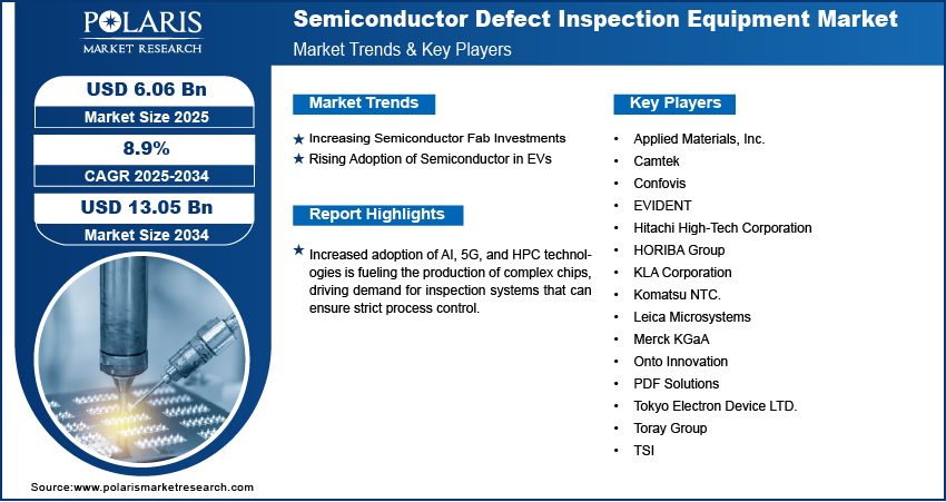
- Applied Materials, Inc.
- Camtek
- Confovis
- EVIDENT
- Hitachi High-Tech Corporation
- HORIBA Group
- KLA Corporation
- Komatsu NTC.
- Leica Microsystems
- Merck KGaA
- Onto Innovation
- PDF Solutions
- Tokyo Electron Device LTD.
- Toray Group
- TSI
Semiconductor Defect Inspection Equipment Industry Developments
March 2025: TASMIT Inc. launched a new glass substrate inspection system within its INSPECTRA series, enhancing defect detection and surface quality assessment for semiconductor wafers.
February 2025: TORAY ENGINEERING Co., Ltd. launched a novel inspection system for large glass substrates in the advanced semiconductor packaging industry, featuring double-sided inspection and internal defect detection.
Semiconductor Defect Inspection Equipment Market Segmentation
By Defect Outlook (Revenue, USD Billion, 2020–2034)
- Crystal Defect Inspection
- Metal Defect Inspection
- Mask/Reticle Defect Inspection
- Others
By Technology Outlook (Revenue, USD Billion, 2020–2034)
- Optical Inspection
- Electron Beam Inspection
- X-ray Inspection
- Others
By Inspection Technique Outlook (Revenue, USD Billion, 2020–2034)
- 2D Inspection Techniques
- 3D Inspection Techniques
- Machine Learning and AI
By Process Stage Outlook (Revenue, USD Billion, 2020–2034)
- Front-End of Line (FEOL)
- Back-End of Line (BEOL)
- Photomask Shops / Reticle Inspection
- Packaging & Assembly
- R&D and Failure Analysis
By End Use Outlook (Revenue, USD Billion, 2020–2034)
- Foundry
- Memory
- Logic
- Integrated Device Manufacturer (IDM)
By Regional Outlook (Revenue, USD Billion, 2020–2034)
- North America
- U.S.
- Canada
- Europe
- Germany
- France
- UK
- Italy
- Spain
- Netherlands
- Russia
- Rest of Europe
- Asia Pacific
- China
- Japan
- India
- Malaysia
- South Korea
- Indonesia
- Australia
- Vietnam
- Rest of Asia Pacific
- Middle East & Africa
- Saudi Arabia
- UAE
- Israel
- South Africa
- Rest of Middle East & Africa
- Latin America
- Mexico
- Brazil
- Argentina
- Rest of Latin America
Semiconductor Defect Inspection Equipment Market Report Scope
| Report Attributes | Details |
| Market Size in 2024 | USD 5.57 billion |
| Market Size in 2025 | USD 6.06 billion |
| Revenue Forecast by 2034 | USD 13.05 billion |
| CAGR | 8.9% from 2025 to 2034 |
| Base Year | 2024 |
| Historical Data | 2020–2023 |
| Forecast Period | 2025–2034 |
| Quantitative Units | Revenue in USD billion and CAGR from 2025 to 2034 |
| Report Coverage | Revenue Forecast, Competitive Landscape, Growth Factors, and Industry Trends |
| Segments Covered |
|
| Regional Scope |
|
| Competitive Landscape |
|
| Report Format |
|
| Customization | Report customization as per your requirements with respect to countries, regions, and segmentation. |
FAQ's
The global market size was valued at USD 5.57 billion in 2024 and is projected to grow to USD 13.05 billion by 2034.
The global market is projected to register a CAGR of 8.9% during the forecast period.
Asia Pacific accounted for the largest revenue share of ~68% due to its dominant role in global chip fabrication, particularly in memory and advanced logic.
A few of the key players in the market are Applied Materials, Inc.; Camtek; Confovis; EVIDENT; Hitachi High-Tech Corporation; HORIBA Group; KLA Corporation; Komatsu NTC.; Leica Microsystems; Merck KGaA; Onto Innovation; PDF Solutions; Tokyo Electron Device LTD.; Toray Group; and TSI.
The crystal defect inspection segment dominated the market in 2024 with ~31% of the revenue share due to rising demand for defect-free silicon substrates used in advanced semiconductor fabrication.
The optical inspection segment held ~35% of the revenue share in 2024 due to its widespread adoption across multiple stages of wafer processing.
Download Sample Report of Semiconductor Defect Inspection Equipment Market
Please fill out the form to request a customized copy of the research report.
