
Extreme Ultraviolet Lithography Market Size, Share, Trends | Report 2026-2034
REPORT DETAILS
Extreme Ultraviolet Lithography Market Summary
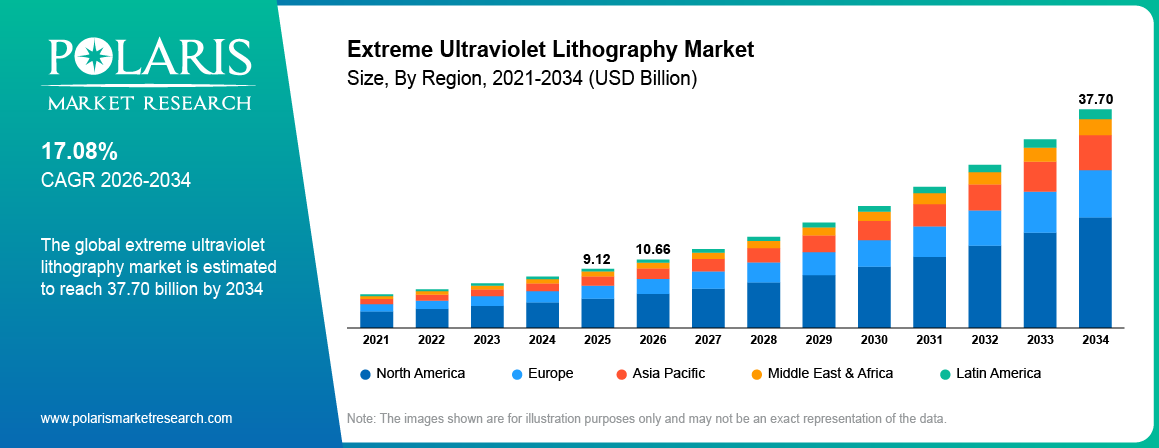
The global extreme ultraviolet lithography market was valued at USD 14.16 billion in 2025 and is projected to reach USD 36.46 billion by 2034, registering a CAGR of 11.08% during the forecast period. Growth of the market is influenced by increasing demand for advanced semiconductor nodes, rising investments in chip manufacturing facilities, and growing adoption of EUV technology for next-generation semiconductor production.
Market Statistics
Extreme Ultraviolet Lithography Market Key Takeaways 2025
- Asia Pacific held the largest share in the market accounting for 38.0% during 2025 due to the presence of leading semiconductor foundries, advanced fabrication facilities, and increasing investments in chip manufacturing infrastructure.
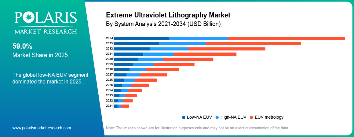
- Low-NA EUV occupied the majority segment share of 59.0% during 2025, mainly due to its established adoption in advanced semiconductor manufacturing processes.
- Logic applications held the largest market share of 52.0% in 2025, owing to increasing demand for advanced processors used in AI, high-performance computing, and electronic devices.
- The optics segment is projected to grow at the fastest CAGR of 16.5% during the forecast period due to increasing demand for advanced optical systems that improve resolution, accuracy, and semiconductor manufacturing efficiency.\
Note: Figures and projections outlined in this report are the result of Polaris Market Research’s proprietary analytical processes, grounded in the latest available datasets and market observation
What is Extreme Ultraviolet (EUV) Lithography?
Extreme ultraviolet (EUV) lithography refers to an innovative semiconductor fabrication process, where light of extremely short wave length is used to form very accurate patterns on semiconductor substrates. This technology allows chip producers to manufacture more compact and efficient semiconductor chips necessary for AI, HPC, and other electronic systems.
Extreme ultraviolet lithography is different from conventional lithography techniques which provides the capability for semiconductor scaling. This market aims at enhancing the efficiency of chip fabrication through use of advanced EUV systems and high-resolution patterning technology.
Source: Polaris Market Research Analysis
Extreme Ultraviolet Lithography Market Driver Impact Analysis
Extreme ultraviolet lithography market is expected to witness a CAGR of 17.08% till 2034 due to the increasing demand for advanced semiconductor manufacturing, expansion of AI applications, and rising investments in semiconductor fabrication facilities. The table below highlights the key factors supporting market growth across major regions.
| Market Driver | Est. CAGR Impact | Geographic Relevance | Impact Timeline |
| Rising demand for advanced semiconductor nodes | +2.3% | Asia Pacific, US, Europe | Medium to long term |
| Increasing investments in next-generation chip manufacturing | +2.0% | Asia Pacific, US | Medium term (2 to 5 years) |
| Technological advancements in High-NA Extreme EUV lithography | +1.8% | Europe, US, Asia Pacific | Short to medium term |
| Expansion of semiconductor fabrication facilities | +1.5% | US, China, Japan, South Korea, Taiwan | Medium term (2 to 4 years) |
| Government incentives for domestic semiconductor production | +1.2% | US, Europe, Japan, South Korea | Medium to long term |
* Indicative estimates based on market context and analyst judgment. Figures reflect relative driver weight, not additive CAGR contributions. Source: Polaris Market Research Analysis.
Extreme Ultraviolet Lithography Market Industry Dynamics
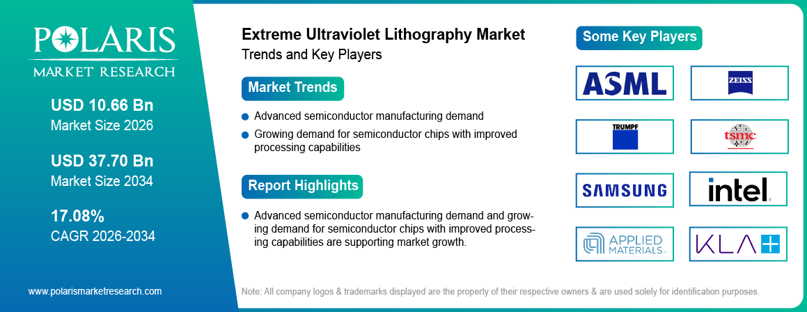
- Advanced semiconductor manufacturing demand are increasing demand for EUV lithography.
- Growing demand for semiconductor chips with improved processing capabilities is driving the market growth.
- High equipment complexity remain a major barrier for EUV lithography technology.
- Semiconductor manufacturing expansion is creating opportunities for EUV lithography market.
Extreme Ultraviolet Lithography Market Drivers, Restraints and Opportunities
What is Driving Extreme Ultraviolet Lithography Market Growth? Advanced Semiconductor Manufacturing Demand
The increasing demand for advanced semiconductor manufacturing is driving the growth of extreme ultraviolet lithography market. EUV lithography enables semiconductor manufacturers to produce smaller and more efficient chips required for AI, cloud computing, consumer electronics, and high-performance computing applications. For instance, in 2026, the Semiconductor Industry Association (SIA) reported that the global semiconductor sales grew to USD 110.5 billion in April 2026 from USD 56.9 billion in April 2025, indicating strong future demand for EUV lithography(Source: semiconductors.org).
How is AI Reshaping the Extreme Ultraviolet Lithography Market?
AI is reshaping the EUV lithography market by increasing the demand for advanced semiconductor chips with improved processing capabilities. AI applications require high-performance processors manufactured using advanced lithography technologies. Computational lithography using AI and other process optimization technologies help manufacturers to achieve greater accuracy, minimize defects, and optimize production processes.
What Challenges Threaten Extreme Ultraviolet Lithography Market Expansion? High Equipment Complexity
High equipment complexity remains a major challenge for the expansion of extreme ultraviolet lithography market. The implementation of the EUV system requires advanced optical elements and light source technology. High prices on EUV equipment limit its wide usage by small semiconductor companies. Moreover, difficulties with the maintenance of equipment and the supply chain serve as another obstacle for the implementation of EUV lithography technology.
What Opportunities Exist in the Extreme Ultraviolet Lithography Market? Semiconductor Manufacturing Expansion
Increasing manufacturing capability of semiconductors is creating opportunities for the extreme ultraviolet lithography industry. Rising investment in semiconductor fabrication plants and growing demands for advanced chips are leading companies to use EUV technology. The government's initiatives of building domestic semiconductor fabrication plants with rising private investments in semiconductor fabrication plants are also contributing to market growth. For instance, in 2024, Tata Electronics announced an investment of USD 2.86 billion to set up a semiconductor plant in Assam, India, showing massive entry of private players in the semiconductor manufacturing industry(Source: tata.com).
Source: Polaris Market Research Analysis
Segment and Regional Leaders at a Glance
According to Polaris Market Research, Asia Pacific leads the market while North America is the fastest-growing region.
- Dominant Region: Asia Pacific
- Fastest-Growing Region: North America
- Largest System Segment: Low-NA EUV
- Largest Application Segment: Logic
- Largest Component Segment: Light source
Segmentation Analysis
The report provides a comprehensive analysis of the extreme ultraviolet (EUV) lithography market by system, application, and component to identify key revenue-generating and high-growth segments.
Extreme Ultraviolet Lithography Market by System
What is the Largest System Segment in the Market?
The Low-NA EUV segment dominated the extreme ultraviolet lithography market with 59.0% share in 2025 due to its established adoption in advanced semiconductor manufacturing processes. Low-NA EUV systems are widely utilized by semiconductor manufacturers for producing advanced chips and supporting high-volume manufacturing requirements.
Which System Segment is Growing Fastest in the Market?
The High-NA EUV segment is projected to grow at the fastest CAGR of 24.4% during the forecast period. Increasing demand for next-generation semiconductor nodes and higher-resolution patterning capabilities is encouraging semiconductor manufacturers to adopt High-NA EUV systems.
Extreme Ultraviolet Lithography Market by Application
Which Application Segment Leads the Market?
Logic applications dominated the extreme ultraviolet lithography market with 52.0% share in 2025 due to increasing demand for advanced processors used in AI, high-performance computing, and electronic devices. EUV lithography enables semiconductor manufacturers to produce smaller and more efficient logic chips with improved performance.
Which Application Segment is Growing Fastest in the Market?
The DRAM application is expected to register the highest CAGR of 16.2% during the forecast period owing to rising demands for high-performing memory solutions, data centers, and AI-based computers. For instance, in 2026, Applied Materials introduced Centura Prime Epi system to accelerate DRAM that boosts memory speed and efficiency while maximizing output within tight fab footprint and supply constraints.
Extreme Ultraviolet Lithography Market by Component
Which Component Segment Leads the Market?
Light source segment led the EUV lithography market with 25.0% share in 2025 owing to its importance in producing the extreme ultraviolet radiation necessary for semiconductor patterning. Highly advanced EUV light source systems facilitate precision-based manufacturing and help in the development of the latest generation semiconductor devices.
Which Component Segment is Growing Fastest in the Market?
The optics segment is projected to grow at the highest CAGR of 16.5% during the forecast period owing to the rising demand for enhanced optical technology which provides better resolution, accuracy, and improved efficiency in semiconductor production. Continuous innovation in EUV optics is supporting the development of advanced lithography platforms.
Segment Summary Table
| Segment | Category | 2025 Status | Forecast CAGR | Key Driver |
| Low-NA EUV | System | Largest share | High | Advanced semiconductor manufacturing |
| High-NA EUV | System | Fastest growing | High | Next-generation chip scaling |
| Logic | Application | Largest share | High | Advanced processor demand |
| DRAM | Technology | Fastest growing | High | Memory semiconductor |
| Light Source | Component | Largest share | High | EUV radiation generation |
| Optics | Component | Fastest growing | High | Precision lithography requirements |
Source: Polaris Market Research Analysis
Source: Polaris Market Research Analysis
Regional Analysis
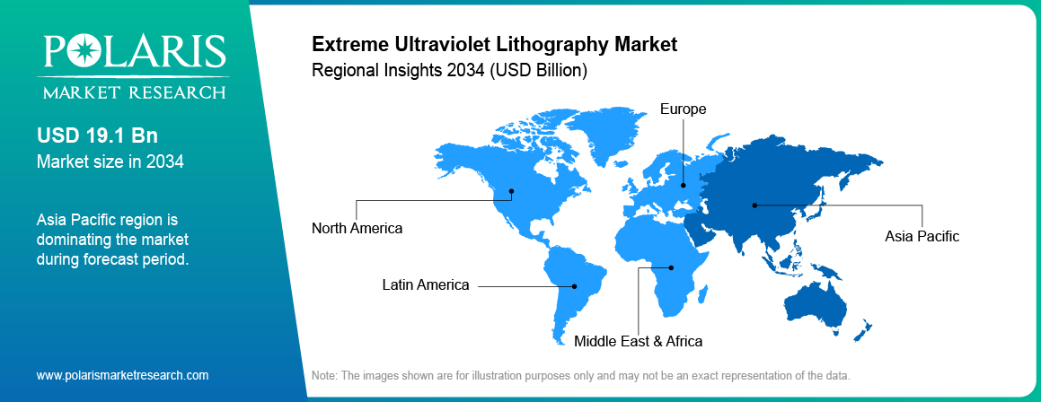
The extreme ultraviolet lithography market demonstrates significant regional variation in terms of semiconductor manufacturing capabilities, research investments, and fabrication infrastructure. Asia Pacific dominates global revenue generation. Europe benefits from strong semiconductor equipment industry, and advanced optical technology capabilities, and North America represents the fastest-growing regional opportunity due to increasing semiconductor manufacturing investments, and growing focus on domestic fabrication capabilities.
Asia Pacific Extreme Ultraviolet Lithography Market Size and Share
Asia Pacific dominated the EUV lithography market with 38.0% share in 2025, due to the presence of leading semiconductor foundries, advanced fabrication facilities, and increasing investments in chip manufacturing infrastructure. India, China, and Japan are becoming major regions for semiconductor and EUV technology manufacturing due to growing demand for AI chips and consumer electronic devices. For example, in 2026, the Indian Ministry of Electronics & IT reported that the total value of electronics goods produced in India reached USD 119.73 billion during 2024-2025, an increase of 600% from 2014-2015(Source: pib.gov.in).
Europe Extreme Ultraviolet Lithography Market Analysis
Europe occupied a significant share of global EUV lithography market valued at 23.0% share in 2025 owing to the presence of a well-developed industry of semiconductor equipment and optics. Germany and the Netherlands are creating a major impact on the EUV lithography market due to their manufacturing and development in semiconductor technology. Growing investments toward next-generation chip manufacturing and semiconductor innovation are further enhancing regional market expansion. For example, the European Commission introduced the European Chips Act in 2023 with more than USD 113.40 billion investment that is expected to support the chips act until 2030, for strengthening the semiconductor manufacturing industry in the region(Source: digital-strategy.ec.europa.eu).
North America Extreme Ultraviolet Lithography Market Growth Rate and Forecast
North America is projected to grow at the fastest CAGR of 15.0% during the forecast period due to increasing semiconductor manufacturing investments, and growing focus on domestic fabrication capabilities. The region benefits from strong presence of technology companies, research institutions, and semiconductor manufacturers. Increasing adoption of AI, high-performance computing, and advanced semiconductor applications is further supporting regional market growth. For instance, in 2026, Nokia announced a multi-year plan to invest USD 4 billion in R&D and manufacturing in the US for AI-ready network connectivity, indicating strong future demand for EUV lithography in the region(Source: nokia.com).
Latin America Extreme Ultraviolet Lithography Market Analysis
Latin America analysis covers Brazil, Mexico, Chile, Colombia, and Argentina. The extreme ultraviolet (EUV) lithography market in the region is influenced by semiconductor industry development, technology investments, supplier presence, and import dependency. Growing demand for advanced electronics and digital infrastructure is further creating opportunities for the market.
Middle East and Africa Extreme Ultraviolet Lithography Market Analysis
Middle East and Africa analysis covers Saudi Arabia, UAE, Israel, South Africa, and Egypt. The regional EUV lithography market growth is supported by increasing technology investments, semiconductor initiatives, and advanced manufacturing development. Market performance depends on investment capacity, supplier availability, import exposure, and adoption of advanced semiconductor technologies.
Source: Polaris Market Research Analysis
Regulatory Heatmap
| Country | Policy Environment | Key Regulations | Market Implication | Trend |
| US | Favorable | Semiconductor manufacturing initiatives; advanced technology investment programs | Supports semiconductor production expansion and advanced technology adoption | Expanding |
| Canada | Neutral | Federal technology initiatives and semiconductor development programs | Creates opportunities with dependency on technology partnerships | Developing |
| Germany | Favorable | European semiconductor framework and national technology programs | Supports advanced manufacturing and regulated semiconductor adoption | Expanding |
| UK | Neutral | Semiconductor strategy and technology innovation programs | Creates opportunities through research and industry collaboration | Stable |
| China | Favorable | Semiconductor industry development policies and localization initiatives | Supports market growth but increases technology ecosystem challenges | Expanding |
| Japan | Favorable | Semiconductor technology programs and advanced manufacturing initiatives | Supports premium semiconductor applications and equipment development | Stable |
| India | Developing | Semiconductor mission and electronics manufacturing programs | Creates long-term growth opportunities through ecosystem development | Developing |
| Australia | Neutral | Standards and technology innovation programs | Supports selective semiconductor technology adoption and research activities | Developing |
Source: Polaris Market Research Analysis
Competitive Landscape and Key Players
The global extreme ultraviolet lithography market is highly concentrated, with competition occurring across EUV lithography systems, semiconductor equipment technologies, optical components, and advanced manufacturing solutions. Key competitive factors include technological capabilities, equipment performance, research investments, manufacturing expertise, and strategic collaborations.
The business environment is rapidly evolving, driven by increasing demand for advanced semiconductor chips, AI applications, and next-generation manufacturing technologies. Partnerships, technology development, and investments in advanced lithography systems continue to remain important strategies for major industry participants.
Competitive Positioning Table
| Company | Est. Market Position | Primary Focus | Geographic Focus | In Report |
| ASML | Top 1 | EUV lithography systems | Global | Yes |
| Carl Zeiss SMT | Top 3 | EUV optical systems | Global | Yes |
| TRUMPF | Top 5 | EUV light sources | Europe | Yes |
| TSMC | Top 5 | Semiconductor manufacturing | Asia Pacific | Yes |
| Samsung Electronics | Top 10 | Advanced semiconductor production | Asia Pacific | Yes |
| Intel | Top 10 | Semiconductor manufacturing | North America | Yes |
* Estimated market positioning based on revenue scale, geographic reach, and service breadth. Not ranked by precise market share percentage. Source: Polaris Market Research Analysis.
Technology and Innovation Landscape 2025-2026
Extreme ultraviolet lithography is advancing through innovations in High-NA EUV systems, advanced optical technologies, improved EUV sources, and semiconductor process optimization. These developments are improving resolution capabilities, production efficiency, and support for advanced semiconductor nodes.
| Technology | Adoption Stage | Key Development | Market Impact |
| High-NA EUV Lithography | Growing deployment | Development of next-generation EUV systems | Enables advanced chip scaling |
| EUV Source Technology | Growing deployment | Improvements in EUV power generation | Enhances productivity |
| Advanced Optical Systems | Growing deployment | Improved precision and imaging performance | Supports higher resolution |
| Computational Lithography | Early commercial deployment | Process optimization technologies | Improves manufacturing efficiency |
Source: Polaris Market Research Analysis
Who Buys Market Research and Why?
The extreme ultraviolet lithography market report helps stakeholders identify growth opportunities, market trends, and competitive positioning.
| Buyer / Investor Type | Primary Use Case | Key Insight Sought | Decision Horizon |
| Semiconductor Foundries | Expansion planning | EUV adoption opportunities | 3-7 years |
| Integrated Device Manufacturers | Technology assessment | Advanced semiconductor trends | 2-5 years |
| Semiconductor Equipment Companies | Product development | Technology requirements | 2-5 years |
| Venture Capital Firms | Investment evaluation | Market potential | 2-5 years |
| Government Agencies | Policy planning | Semiconductor ecosystem growth | 5-10 years |
Source: Polaris Market Research Analysis
What are the Barriers to Entering the Market?
- High Capital Requirements: EUV lithography systems require massive investment owing to their complex design and advanced engineering.
- Technology Complexity: Development of EUV systems need expertise in optics, semiconductor manufacturing, advanced materials, and advanced manufacturing process.
- Supply Chain Limitations: Difficulties in obtaining specialized components and advanced manufacturing capabilities creates challenges for new companies.
- Intellectual Property Barriers: Extensive patents and technology make it difficult for newcomers in the industry.
- Manufacturing Challenges: Maintaining productivity, improving accuracy, and obtaining high wafer yields remain the challenges.
- Skilled Workforce Requirement: Highly skilled technical manpower is needed in advanced semiconductor manufacturing.
- Infrastructure Requirements: EUV manufacturing requires advanced infrastructure, facilities, and equipment.
Premium Insights and Forward Outlook
AI-Driven Semiconductor Manufacturing Ecosystem
The implementation of AI in semiconductor manufacturing processes is becoming a key factor affecting the growth of the EUV lithography market. Process optimization, computational lithography, and defect detection using AI technology are becoming crucial for efficient production processes.
Advanced Semiconductor Scaling Expansion
Rising demand for compact, fast and efficient semiconductors is creating opportunities for EUV lithography technology. AI, supercomputers and electronics devices require semiconductors produced through advanced lithography processes. Semiconductor firms are making investments in EUV systems to facilitate the production of future generation chips.
Cost Benchmarking Table
| Product | Est. Price Range | Key Cost Driver | Complexity Tier |
| Low-NA EUV | USD 50,000 to USD 250,000 | Specification and validation burden | Mid to high |
| High-NA EUV | USD 75,000 to USD 400,000 | Technology integration | High |
| Logic | USD 25,000 to USD 150,000 | Deployment and service scope | Mid |
| Light source | USD 100,000 to USD 750,000 | Scale and compliance documentation | High |
Source: Polaris Market Research Analysis
Key Players
- ASML Holding N.V.
- Carl Zeiss SMT GmbH
- TRUMPF GmbH
- TSMC
- Samsung Electronics Co. Ltd.
- Intel Corporation
- Applied Materials Inc.
- KLA Corporation
- Lam Research Corporation
- Tokyo Electron Limited
- Nikon Corporation
- Canon Inc.
Industry Developments
- May 2026: Tata Electronics and ASML signed a Memorandum of Understanding (MoU) to ramp-up Tata Electronics’ upcoming 300 mm semiconductor fabrication facility in Gujarat(source tata.com).
- April 2026: Tokyo Electron installed its CLEAN TRACK LITHIUS Pro DICE 300mm wafer coater/developer system at NY Creates’ Albany NanoTech Complex to support next-generation semiconductor manufacturing(source: governor.ny.gov).
- February 2026: Qnity Electronics introduced its Eon EUV photoresist product family to expand its offerings for extreme ultraviolet lithography(source: qnityelectronics.com).
Market Segmentation
By System Outlook (Revenue, USD Billion, 2021–2034)
- Low-NA EUV
- High-NA EUV
- EUV metrology
By Application Outlook (Revenue, USD Billion, 2021–2034)
- Logic
- DRAM
- Foundry services
By Component Outlook (Revenue, USD Billion, 2021–2034)
- Light source
- Optics
- Photoresist
- Masks
By Regional Outlook (Revenue, USD Billion, 2021-2034)
- North America
- US
- Canada
- Europe
- Germany
- France
- UK
- Italy
- Spain
- Netherlands
- Russia
- Rest of Europe
- Asia Pacific
- China
- Japan
- India
- Malaysia
- South Korea
- Indonesia
- Australia
- Vietnam
- Rest of Asia Pacific
- Middle East & Africa
- Saudi Arabia
- UAE
- Israel
- South Africa
- Rest of Middle East & Africa
- Latin America
- Mexico
- Brazil
- Argentina
- Rest of Latin America
Report Scope
| Report Attributes | Details |
| Market Size in 2025 | USD 14.16 Billion |
| Market Size in 2026 | USD 15.70 Billion |
| Revenue Forecast by 2034 | USD 36.46 Billion |
| CAGR | 11.08% from 2026 to 2034 |
| Base Year | 2025 |
| Historical Data | 2021–2024 |
| Forecast Period | 2026–2034 |
| Quantitative Units | Revenue in USD Billion and CAGR from 2026 to 2034 |
| Report Coverage | Revenue Forecast, Competitive Landscape, Growth Factors, and Industry Trends |
| Segments Covered |
|
| Regional Scope |
|
| Competitive Landscape |
|
| Report Format |
|
| Customization | Report customization as per your requirements with respect to countries, regions, and segmentation. |
Extreme Ultraviolet Lithography Market FAQ's
• The global market size was valued at USD 14.16 Billion in 2025 and is projected to grow to USD 36.46 Billion by 2034.
• Asia Pacific dominated the market with 38.0% share in 2025 owing to strong semiconductor manufacturing and rising chip fabrication investments.
• The Low-NA EUV segment accounted for the largest market share of 59.0% in 2025.
• Key participants include ASML Holding N.V., Carl Zeiss SMT GmbH, TRUMPF GmbH, TSMC, Samsung Electronics Co. Ltd., and others.
• Some of the key drivers include the advanced semiconductor manufacturing demand, growing demand for semiconductor chips with improved processing capabilities, and semiconductor manufacturing expansion.
• Logic application held the largest share of 52.0% among application segments in 2025.
Download Sample Report of Extreme Ultraviolet Lithography Market
Please fill out the form to request a customized copy of the research report.


