
Reports

U.S. Wet Process Equipment Market Growth, Trends, Industry Report, 2025-2034
REPORT DETAILS
REPORT DETAILS
ABOUT THIS REPORT
Market Statistics
Overview
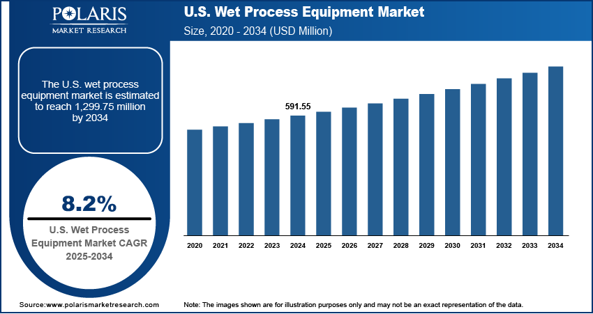
The U.S. wet process equipment market size was valued at USD 591.55 million in 2024, growing at a CAGR of 8.2% from 2025 to 2034. Federal initiatives and incentives under programs such as the CHIPS and Science Act are accelerating efforts to bring semiconductor manufacturing back to the U.S., driving demand for advanced wet process equipment to support new fabrication facilities and ensure domestic production capacity.
Key Insights
- The cleaning systems segment dominated the market with ~43% of the revenue share in 2024, as strong demand for wafer cleanliness across semiconductor fabrication lines is elevating the use of advanced cleaning systems.
- The automatic segment held ~61% of the revenue share in 2024 due to rising demand for production efficiency and minimal operator intervention.
- The semiconductor segment held the largest revenue share of ~73% in 2024 due to increasing investments in domestic semiconductor manufacturing.
Industry Dynamics
- Growing demand for advanced semiconductors in AI, electric vehicles, and 5G is driving investments in the U.S. wet process equipment industry.
- Expansion of semiconductor fabs in the U.S. is boosting demand for high-precision cleaning and etching tools.
- Opportunity lies in developing eco-friendly, water- and chemical-efficient wet processing technologies to meet sustainability and regulatory requirements.
- High capital costs and complex maintenance hinder the U.S. wet process equipment market growth.
Market Statistics
- 2024 Market Size: USD 591.55 million
- 2034 Projected Market Size: USD 1,299.75 million
- CAGR (2025–2034): 8.2%
To Understand More About this Research: Download Sample Report
The wet process equipment market focuses on the production and sale of systems used in semiconductor and microelectronics manufacturing for cleaning, etching, stripping, and developing silicon wafers. These systems use liquid chemicals to treat wafers during various steps of fabrication, ensuring precision and defect-free processing. Wet process equipment is critical in advanced semiconductor nodes, photovoltaics, micro-electro-mechanical systems (MEMS), LED fabrication, and packaging applications. Major semiconductor foundries are investing in new fabrication plants across states such as Texas and Arizona. These expansions require state-of-the-art wafer cleaning and etching tools, boosting the market for wet process equipment as fabs scale up production volume and adopt new node technologies.
Increased focus on domestic production of secure electronics for military and aerospace applications is pushing the integration of advanced semiconductor packaging and processing. This creates demand for reliable wet processing tools that meet high-precision and contamination-control standards in sensitive defense environments. Moreover, the rising need for high-performance computing, AI, and 5G infrastructure is pushing U.S. firms to expand logic and memory chip capabilities. These processes rely heavily on wet benches and chemical processing equipment to ensure low-defect, high-yield wafer fabrication.
Drivers and Opportunities
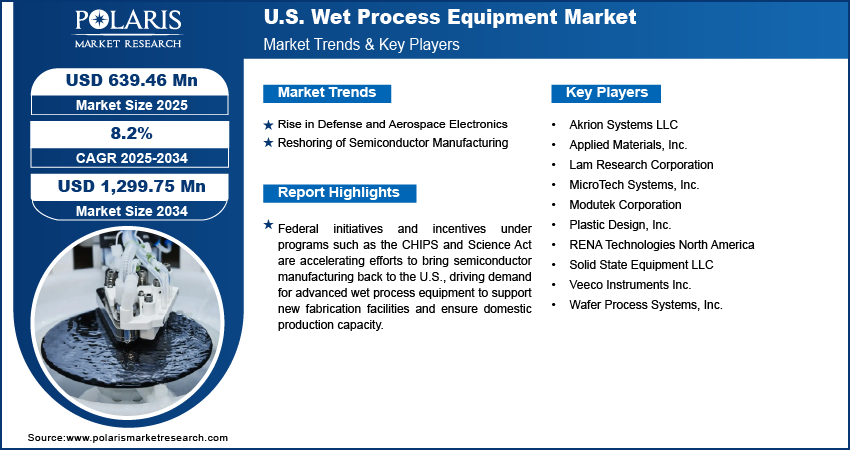
Rise in Defense and Aerospace Electronics: Growing emphasis on national security and supply chain resilience is strengthening the U.S. push to localize the production of defense-grade electronics. According to the Aerospace Industries Association, in 2023, the U.S. aerospace and defense sector reported sales surpassing USD 955 billion, reflecting a 7.1% increase from 2022. Defense and aerospace applications require semiconductors that meet strict performance, durability, and reliability standards. Wet process equipment plays a key role in ensuring high-purity wafer cleaning, precise etching, and contamination-free processing, which are essential for such critical components. Increasing demand for rad-hard chips, advanced packaging, and secure communications infrastructure is encouraging investments in domestic semiconductor fabs tailored for defense needs. This is driving the adoption of customized wet processing systems designed for sensitive environments where precision and cleanliness are non-negotiable.
Reshoring of Semiconductor Manufacturing: National-level policies such as the CHIPS and Science Act are reshaping the U.S. semiconductor ecosystem by incentivizing local production and reducing reliance on foreign supply chains. The Department of Commerce's CHIPS Incentives program has entered into preliminary agreements with 15 companies spanning 15 states, allocating in excess of USD 30 billion in direct funding along with approximately USD 25 billion in loans to support semiconductor manufacturing initiatives. Leading manufacturers are establishing and expanding fabrication plants across the country, creating a surge in demand for high-efficiency wet process equipment to support wafer cleaning, development, and chemical treatments. These tools are vital for meeting quality, throughput, and yield goals in newly built fabs. Reshoring efforts are also encouraging partnerships between domestic toolmakers and foundries to ensure equipment customization and supply security, reinforcing the wet processing market as a foundational part of U.S. chip manufacturing growth.
Segmental Insights
Product Type Analysis
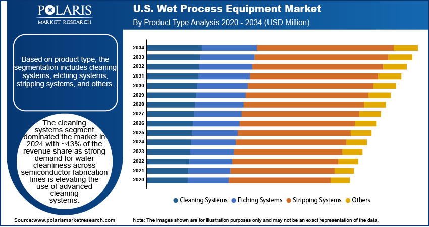
Based on product type, the U.S. wet process equipment market segmentation includes cleaning systems, etching systems, stripping systems, and others. The cleaning systems segment dominated the market with ~43% of the revenue share in 2024, as strong demand for wafer cleanliness across semiconductor fabrication lines is elevating the use of advanced cleaning systems. Fabrication processes require particle-free wafers to maintain high yields, particularly in advanced nodes. Cleaning tools play a crucial role in removing photoresist residues, chemical contaminants, and metal particles without damaging delicate structures. Major U.S. fabs continue to invest in high-throughput, fully automated cleaning platforms integrated with real-time monitoring features. The emphasis on contamination control, particularly in front-end processing, has reinforced the dominance of cleaning systems in the wet process equipment segment across the country’s expanding fab landscape.
The stripping systems segment is expected to register the highest CAGR from 2025 to 2034, as rising demand for advanced packaging and back-end wafer processing is encouraging fabs to adopt more efficient and residue-free photoresist stripping solutions. Complex chip architectures involving 3D ICs and heterogeneous integration require precise stripping steps to maintain interconnect performance and layer integrity. U.S.-based foundries are expanding backend capabilities, prompting demand for wet stripping systems that offer low-temperature chemistries, reduced substrate damage, and compatibility with next-gen materials. This trend is likely to continue as more players adopt advanced lithography nodes and materials that require high-performance, selective resist removal methods throughout the production cycle.
Type Analysis
In terms of type, the segmentation includes automatic, semi-automatic, and manual. The automatic segment held ~61% of the revenue share in 2024, due to demand for production efficiency and minimal operator intervention. These tools deliver superior repeatability, real-time process control, and minimal human error, all of which are critical for maintaining high yields and uptime. Equipment manufacturers are enhancing automation with robotics, AI-driven process monitoring, and closed-loop chemical management to meet evolving standards in advanced manufacturing. The adoption of smart fabs and Industry 4.0 practices is pushing preference toward automatic systems, which enable scalable, cleanroom-compatible integration and seamless transition between different wafer sizes or chemistries.
The semi-automatic segment is expected to register the highest CAGR from 2025 to 2034 due to mid-size and specialty fabs focusing on R&D and low-volume production are investing in semi-automatic wet benches to retain flexibility while optimizing cost. These systems offer better process visibility and manual control while still benefiting from some automation elements such as chemical dosing and bath temperature regulation. The rise in prototyping of compound semiconductors, GaN and SiC devices, and other non-standard wafers in the U.S. is increasing the need for semi-automated tools that allow greater customizability. Universities and research-focused institutions also contribute to this demand, where full automation is not always cost-justified or necessary.
Application Analysis
In terms of application, the segmentation includes semiconductor, MEMS, solar, and others. The semiconductor segment held the largest revenue share of ~73% in 2024 due to increasing investments in domestic semiconductor manufacturing. The resurgence of local chip production across logic, memory, and analog devices is dependent on high-precision tools for wafer cleaning, etching, and development stages. Wet benches are essential across both front-end and back-end processing to maintain cleanliness, critical dimension control, and defect reduction. Federal support programs and commercial initiatives are fueling capacity expansion projects, many of which are outfitted with innovative wet processing systems optimized for advanced nodes. The sector’s capital intensity ensures continuous equipment upgrades, reinforcing this application segment’s leadership.
The MEMS segment is expected to register the highest CAGR from 2025 to 2034, as expanding applications in automotive electronics, biomedical devices, and industrial IoT are stimulating MEMS device fabrication in the U.S. These components require customized wet process steps, especially during wafer thinning, surface micromachining, and cavity formation. Fabrication facilities dedicated to sensors, actuators, and RF MEMS increasingly require compact and modular wet benches that can handle diverse chemistries while ensuring batch uniformity. Growth in demand for wearable technology and next-generation automotive safety features is further increasing investments in MEMS R&D and volume production. This dynamic is set to accelerate the adoption of wet processing solutions tailored for microscale device engineering.
Key Players & Competitive Analysis
The U.S. wet process equipment market is characterized by ongoing innovation and strategic repositioning among key players, who aim to meet the evolving needs of the semiconductor and advanced electronics industries. Industry analysis reveals a clear shift toward customization and high-throughput automation, with manufacturers focusing on modular systems and real-time process monitoring. Market expansion strategies include strengthening domestic manufacturing capabilities and expanding service networks near fabrication clusters. Joint ventures and strategic alliances are emerging to integrate specialized chemistries and robotics into wet benches. Mergers and acquisitions continue to streamline portfolios, enhance product depth, and support post-merger integration of new technologies. Companies are investing heavily in R&D to advance wafer-level cleaning, etching, and stripping capabilities aligned with sub-5nm and heterogeneous integration requirements. Technological advancements such as AI-enabled process control, chemical recycling systems, and advanced material compatibility are shaping competitive differentiation. The market remains dynamic as U.S. policy pushes for reshoring and next-generation chip manufacturing capacity.
Key Players
- Akrion Systems LLC
- Applied Materials, Inc.
- Lam Research Corporation
- MicroTech Systems, Inc.
- Modutek Corporation
- Plastic Design, Inc.
- RENA Technologies North America
- Solid State Equipment LLC
- Veeco Instruments Inc.
- Wafer Process Systems, Inc.
U.S. Wet Process Equipment Industry Developments
June 2025: Applied Materials, Inc. and CEA-Leti collaborated to enhance specialty semiconductor innovation. Through a new memorandum of understanding (MoU), they will expand their joint lab to develop advanced materials engineering solutions addressing infrastructure challenges in AI data centers.
April 2025: Veeco Instruments Inc. announced that its WaferStorm and WaferEtch platforms have received U.S. IDM qualification for two new applications in the Advanced Packaging sector.
U.S. Wet Process Equipment Market Segmentation
By Product Type Outlook (Revenue, USD Million, 2020–2034)
- Cleaning Systems
- Etching Systems
- Stripping Systems
- Others
By Type Outlook (Revenue, USD Million, 2020–2034)
- Automatic
- Semi-automatic
- Manual
By Application Outlook (Revenue, USD Million, 2020–2034)
- Semiconductor
- MEMS
- Solar
- Others
U.S. Wet Process Equipment Market Report Scope
| Report Attributes | Details |
| Market Size in 2024 | USD 591.55 million |
| Market Size in 2025 | USD 639.46 million |
| Revenue Forecast by 2034 | USD 1,299.75 million |
| CAGR | 8.2% from 2025 to 2034 |
| Base Year | 2024 |
| Historical Data | 2020–2023 |
| Forecast Period | 2025–2034 |
| Quantitative Units | Revenue in USD million and CAGR from 2025 to 2034 |
| Report Coverage | Revenue Forecast, Competitive Landscape, Growth Factors, and Industry Trends |
| Segments Covered |
|
| Competitive Landscape |
|
| Report Format |
|
| Customization | Report customization as per your requirements with respect to countries, regions, and segmentation. |
FAQ's
The U.S. market size was valued at USD 591.55 million in 2024 and is projected to grow to USD 1,299.75 million by 2034.
The U.S. market is projected to register a CAGR of 8.2% during the forecast period.
A few of the key players in the market are Akrion Systems LLC; Applied Materials, Inc.; Lam Research Corporation; MicroTech Systems, Inc.; Modutek Corporation; Plastic Design, Inc.; Rena Technologies North America; Solid State Equipment LLC; Veeco Instruments Inc.; and Wafer Process Systems, Inc.
The cleaning systems segment dominated the market in 2024 with ~43% of the revenue share due to strong demand for wafer cleanliness across semiconductor fabrication lines is elevating the use of advanced cleaning systems.
The automatic segment held ~61% of the revenue share in 2024 due to demand for production efficiency and minimal operator intervention.
Download Sample Report of U.S. Wet Process Equipment Market
Please fill out the form to request a customized copy of the research report.
