
Electronic Design Automation Market Size, Share, Trends & Forecast, 2026–2034
REPORT DETAILS
Electronic Design Automation Market Summary
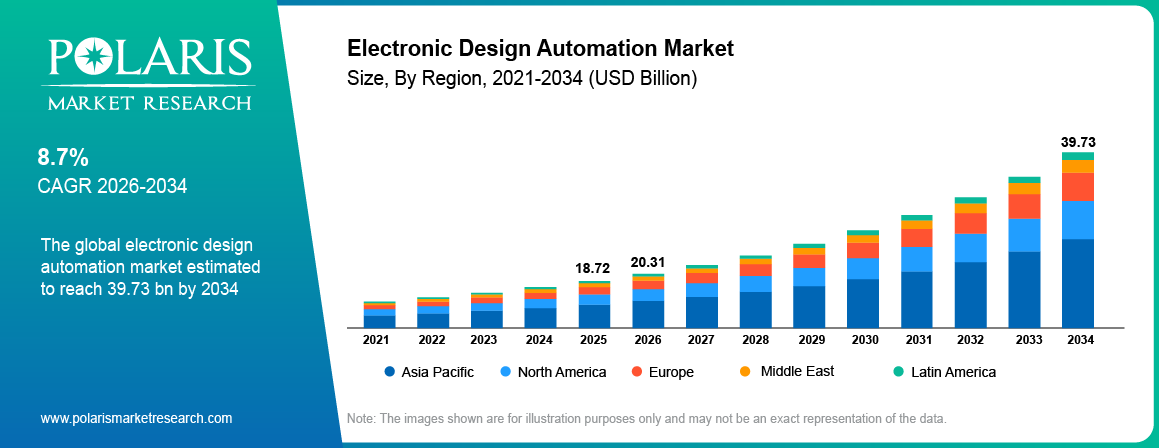
The electronic design automation market was valued at USD 18.72 billion in 2025. The market is projected to grow at a CAGR of 8.7% between 2026 and 2034. Increased demand for advanced chips for artificial intelligence accelerators and new communication systems drives the electronic design automation market growth. Rising complexity of chip designs has also created a need for advanced EDA solutions.
Market Statistics
Electronic Design Automation Market Key Takeaways
- North America led the global electronic design automation market with an 43.86% share in 2025. The presence of a strong semiconductor ecosystem in emerging economies contributes to the regional dominance.
- Asia Pacific is projected to grow at an 11.27% CAGR. Favorable government initiatives and investments in American semiconductor manufacturing drive market growth in the region.
- By product category, the semiconductor intellectual property (IP) segment is projected to grow at an 10.78% CAGR. This is owing to the shift towards heterogeneous chiplet-based designs.
- By deployment mode, the on-premises segment led with an V share in 2025. This is because companies prefer keeping sensitive data and proprietary blueprints on local servers.
- By workflow stage, the physical design tools segment held an 30.84% electronic design automation market share in 2025. This is because translating complex AI chips into microscopic sub-5nm layouts requires massive computational power.
- By end user, the automotive segment is projected to account for an 11.84% CAGR. The shift towards electric vehicles (EVs) drives the rapid growth of the segment.
Note: Figures and projections outlined in this report are the result of Polaris Market Research’s proprietary analytical processes, grounded in the latest available datasets and market observations.
What Is Electronic Design Automation (EDA)?
Electronic design automation refers to software used to support electronic design. It assists in designing and testing semiconductor products before they can be manufactured. EDA is commonly used in the semiconductor design automation market. It also plays a critical role in the chip design software market.
How Electronic Design Automation Works?
EDA design flow consists of eight key phases. Every phase makes the design ready for the next phase.
System specification: In this step, engineers specify the chip’s performance, power, and functional specifications.
RTL design: The behavior of the circuit is specified by means of RTL code.
Design verification: At this phase, engineers verify the correct functioning of the design before its layout.
Logic synthesis: The RTL description is translated to a gate-level netlist.
Place and route: The circuit’s elements are placed and routed in the physical design process.
Timing closure and sign-off: Engineers perform the timing and power checks of the design versus design goals.
Tape-out: The design passes the manufacturing phase checks and is then taped out.
Fabrication, testing, and validation: The chip is fabricated and tested to verify its functionality. Design for test methods support testing post-fabrication.
AI Impact on the Electronic Design Automation Market
AI is transforming the way that EDA tools help to develop chips. This transformation is evident in verification, physical design, and workflow automation. The above trends are broadening the application of artificial intelligence across the semiconductor design automation market.
AI-Assisted Optimization and Verification
AI is being applied to improve design exploration and verification. Cadence uses its JedAI platform to integrate design data and leverage AI in various design flows (source: cadence.com). Synopsys is introducing AI-enabled functionality for physical design and design closure as well. Such technologies can be used by designers to increase design exploration opportunities in existing design flows.
Agentic AI Chip Design (2026)
Agentic AI chip design has become a visible focus in 2026. DAC 2026 included dedicated research areas for agentic AI in synthesis, physical design, verification, and design-flow automation. (source: dac.com)
Siemens introduced self-verifying agentic AI workflows for semiconductor and PCB design at DAC 2026. The workflows combine AI agents with physics-based EDA software to validate results during the design process (source: siemens.com).
Other 2026 developments also show the move toward autonomous workflows. Agentrys raised $24.5 million in August 2026 to expand its agentic chip-design platform. Its platform targets verification and physical design workflows (source: businesswire.com).
LLM-Assisted RTL and Generative Design
Large language models are being used to support hardware design tasks. This includes generating or analyzing RTL from natural-language instructions. NVIDIA highlighted AI-driven hardware code generation at DAC 2026. The conference also included work on generative design and AI-based chip design workflows (source: nvidia.com). These developments are contributing to the emerging generative AI EDA tools and LLM chip design segments.
AI-Native EDA Startups
New companies are developing EDA platforms around AI from the start. ChipAgents raised an additional $60 million in July 2026 to develop artificial intelligence agents for use in designing and verifying chips. CaretEDA also announced an AI-native EDA platform covering simulation, synthesis, verification, and physical synthesis.
These developments are adding new approaches to the chip design software market. They also show how AI in chip design is moving beyond individual tool features toward broader workflow automation.
Chiplets, 3D ICs and Advanced Packaging: The New EDA Design Frontier
Chiplet-based architectures are changing how semiconductor designs are planned and verified. Packaging now has a closer connection with chip design. This shift is increasing the need for EDA tools that can handle multi-die systems and advanced package structures. Chiplet design software and 3D IC EDA tools support this shift.
Multi-Die Design and Verification Challenges
Multi-die systems bring new verification requirements. Engineers must account for connections between dies and the behavior of the complete assembly. Thermal effects can also spread across closely placed chiplets. Mechanical stress adds another design concern. Modern tools can analyze these effects together with electrical behavior. Siemens, for example, offers Calibre 3DStack, Calibre 3DThermal, and Calibre 3DStress for 3D IC verification.
Substrates, Interposers and Package Co-Design
Advanced designs require closer coordination between dies, glass interposers, and substrates. Interposers can connect various chiplets inside the same package. Engineers also need to consider routing and signal integrity even at the packaging level. Cadence and Siemens offer processes that link chiplet design planning with packaging and substrate design. This capability supports advanced packaging design tools and substrate co-design flows.
Electronic Design Automation Market Dynamics
The electronics design automation market is influenced by changes in the complexity of chip design, semiconductor production processes, and usage of specific-purpose processors. Other industry drivers include new developments in design technology and efficiency of the development process.
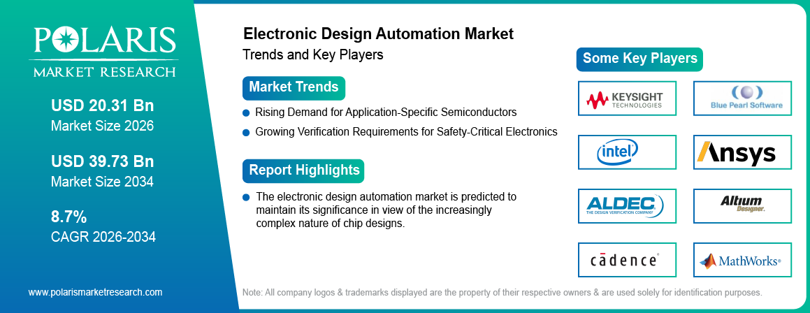
Driver : Rising Demand for Application-Specific Semiconductors
Semiconductor companies are producing more chips that meet the requirements of particular products. Custom chips can be made for specific workloads or system architectures. Such an approach helps companies gain control over the functionality of the chips. This also boosts the need for software that is responsible for modeling and verification of these chips before they are made. EDA tools can assist with this at any stage of chip development. This shift is also reaching car manufacturers, as electronics in cars become more specific. In September 2026, Tata Consultancy Services launched design services for custom system-on-chip in cars by automotive OEMs and semiconductor companies. This includes designing, verification, and validation of the chip (source: tcs.com). Such developments reflect the broader move towards application-specific silicon. They generate more demand for EDA tools for custom semiconductor development.
Driver : Growing Verification Requirements for Safety-Critical Electronics
The needs for verification have become stricter as electronic devices perform tasks that are sensitive in terms of safety. Semiconductor chips are required to pass very high safety requirements to be included in any safety-critical system. This has led to deeper checks of any possible errors and failure scenarios. It has also increased the amount of verification effort necessary before the chip reaches production. As reported by Siemens EDA and Wilson Research Group in September 2026, only 5 percent of respondents among IC and ASIC designers had a first-silicon success rate in 2026. In comparison, the success rate was 14.4 percent in 2024. According to the study, changes in the verification environment were attributed to changes in system complexity and increased safety and assurance needs (source: siemens.com). These factors are contributing to the need for electronic design automation market tools that can perform fault analysis and verification of semiconductors.
Driver : Expansion of Fabless Semiconductor and Design Startup Activity
An increasing number of firms are entering semiconductor design without developing their own manufacturing capacity. Fabless startups can concentrate on design while getting chips manufactured in external foundries. This model reduces the amount of heavy investment in manufacturing facilities. At the same time, it increases the requirement for EDA software during chip design. Government support is helping more startups enter this field. According to an update by the Indian government in August 2026, the DLI-supported firms have already raised more than $100 million and completed 35 design tape-outs. Also, the update notes that these firms have engaged in various commercial and strategic semiconductor design activities (source: pib.gov.in). Therefore, more fabless startups mean more organizations needing EDA software for chip design. This, in turn, contributes to the electronic design automation market expansion.
Challenges and Restraints : High Costs and Complexity in EDA Adoption
The use of EDA can prove to be challenging for businesses with a restricted budget for design. The software license can become costly due to the use of various software programs in the development process. It can also be challenging to find engineers who have expertise in designing and verifying complex chips. The chips need to undergo a lengthy process of verification before they can be put into production. Design at advanced process nodes increases complexity because technical specifications become more demanding. The integration of tools may lead to challenges if there are inconsistencies in data and workflow across different systems. The design team may take extra time trying to solve such challenges. Safeguarding intellectual property becomes another challenge that limits how firms can share their data with outside systems.
Opportunities : Expanding EDA Access for Smaller Design Firms
Cloud-based delivery models can help EDA tools become accessible for small semiconductor companies. Teams can use computing power as needed without building significant internal computing infrastructure. Cloud-based delivery models also provide flexibility and lower the entry cost for using advanced design tools. This could be advantageous for startups pursuing more advanced chip designs. EDA suppliers have the choice of developing tools that target some specific phase in the design process or some specific need. This flexibility enables smaller teams to have access to advanced simulation and verification facilities without having to purchase the whole software toolkit. The growing interest in semiconductor design is expected to generate more customers for EDA suppliers.
Opportunities : Growth of Sovereign and AI-Native EDA Ecosystems
Government-backed semiconductor programs are creating opportunities to enhance chip design domestically. EDA software available through shared access can let startups, universities, and research institutions participate in local semiconductor programs. These programs will also incentivize firms to create intellectual property in their own market. At the same time, native EDA platforms for AI are generating innovative solutions for chip design. These technologies can automate certain engineering processes and facilitate the transition between different stages of designing chips. New EDA vendors can build products on these technologies without altering their software architecture.
Technology Trends and Advancements
Multiphysics and Digital Twin: Chip design now requires closer attention to heat and signal behavior. Multiphysics simulation brings these checks into the design process. Digital twins add a virtual view of how a chip may behave in operation.
Quantum Chip Design: Quantum hardware is opening a separate area for design automation. Quantum chip design requires simulation methods suited to quantum devices. EDA vendors are beginning to address these requirements through specialized design workflows.
Advanced Verification: More complex designs have little room left for mistakes during the physical fabrication process. Therefore, the process of verification takes longer and consumes more computing power. More elaborate verification is becoming common at earlier stages of the design process.
Sub-3 nm Sign-Off: Sub-3 nm designs have stricter constraints on how the chip operates. Timing and power analysis are required for sub-3 nm sign-off. Moreover, EDA software needs to account for foundry constraints in the form of an updated process design kit (PDK).
Market Segmentation Analysis
By Product Category
The computer-aided engineering (CAE) segment accounted for the largest share of 31.27% in 2025. CAE software is employed to evaluate electronic designs prior to going into manufacturing. Computer-aided engineering software can assist in simulation and analysis in the development phase of the product. This requirement becomes even more crucial as semiconductor designs are becoming increasingly complicated. The application of CAE software is for products designed with SoC, ASIC, and FPGA architectures. CAE software is helpful in detecting any problems in the performance of designs in their initial stages. In addition, CAE software can help minimize changes in the subsequent stages of design. The increase in simulations has been instrumental in driving demand for this type of software within the EDA software market. CAE also facilitates analysis of electronics before manufacturing. Such applications are helping the segment maintain its dominant position.
The semiconductor intellectual property (IP) segment is projected to witness an 10.74% CAGR. Semiconductor intellectual property refers to pre-fabricated circuit blocks that can be reused in the design of the chip. Such blocks can save time while creating semiconductor designs. They are frequently embedded in the SoC structure for products with certain requirements. In addition, the complexity of today’s chips is driving demand. Reusable IP may assist design engineers in eliminating the need to create circuits from scratch. It is especially useful for those companies that work on creating semiconductor products that have a tight schedule. Thus, the increasing application of semiconductor intellectual property (SIP) is fueling demand in the EDA market. Adoption across ASIC and other specialized chip designs is also contributing to segment growth.
| Product category | What it covers | Main demand driver |
| Computer-aided engineering (CAE) | Simulation and analysis: thermal, electromagnetic, signal integrity, multiphysics | Multi-die reliability, automotive and aerospace safety |
| IC physical design and verification | Floorplanning, place and route, timing closure, DRC/LVS, sign-off | Advanced-node complexity, AI accelerators |
| Semiconductor intellectual property (SIP) | Pre-verified processor, memory and interface blocks | Chiplets, faster time-to-market, reuse |
| PCB and multi-chip module (MCM) | Board and module layout, schematic capture, signal integrity | Consumer, automotive and industrial electronics |
| Services | Design services, integration, tool support, training | Talent shortage, outsourced design |
Source: Polaris Market Research Analysis
EDA Market by Workflow Stage
The physical design tools segment accounted for an 30.84% electronic design automation market share in 2025. The need for such tools is fuelled by the increasing complexity of modern chip designs. The semiconductor industry is facing challenges of increased transistor density and tight design rules. This raises the demand for tools capable of handling physical design in greater detail. Place and route tools are becoming increasingly vital as chip area becomes scarcer. Demand is also supported by stricter requirements for timing closure and sign-off. Modern designs need more elaborate verification before being sent out to tape. The increasing trend towards advanced semiconductor nodes adds to this pressure. This is further contributing to the dominance of physical design tools within the EDA market segment.
The front-end design tools segment is projected to grow at an 10.68% CAGR. The growth is facilitated by the growing number of semiconductor designs that are designed specifically to meet certain performance criteria. These developments involve considerable effort before the actual physical implementation. There is an increasing demand for the RTL design and logic synthesis tools because of the growth in complexity of digital architectures. An increased emphasis on design verification is also driving the adoption of front-end tools. Early design testing is becoming increasingly important because companies want to avoid costly mistakes later in development. The growing importance of front-end tools is driven by the increasing number of fabless companies and startups implementing their custom chips. As a result, growth in semiconductor design activities is expanding the customer base for this market segment.
By Deployment Mode
The on-premises segment held the largest electronic design automation market share of 58.74% in 2025. This positioning is supported by the needs of semiconductor companies with large design environments. The on-premises installation allows them to have full control over software and computation data resources. This is vital, especially when designs include intellectual property. This also lets companies integrate EDA software with their existing engineering systems. Existing design teams are likely to already have hardware resources and supporting systems set up within the company. This makes on-premises installation a viable option for lengthy projects. Another area where there is constant demand for EDA software comes from those who need regular access to high-performance computing systems. All these factors contribute to the leading position of the segment.
The cloud-based segment is projected to grow at an 11.36% CAGR. This growth is supported by changes in how semiconductor teams handle intensive computing workloads. For instance, cloud computing resources can be deployed to assist projects that need extra computing power at certain phases. The use of burst compute makes it possible for teams to deal with high workloads without the need to add new infrastructure for the company. The cloud can also support collaboration among design teams in various locations. EDA hybrid cloud offers another alternative through integration of internal and external computing power. This approach could be useful for organizations that want to keep core workloads within the organization while outsourcing some tasks to the cloud. EDA software and cloud computing resources can be used flexibly as EDA-as-a-service. These developments are broadening the role of cloud-based deployment within the EDA market.
| Factor | On-premises | Cloud-based | Hybrid (burst to cloud) |
| Cost model | Capital-heavy hardware plus licenses | Pay-as-you-go subscription | Licenses on-premises, compute credits in cloud |
| Scalability | Fixed capacity | Elastic | Elastic for regression and verification peaks |
| IP security posture | Strongest control | Depends on provider and controls | Golden IP stays local |
| Typical users | Tier-1 fabless firms, IDMs, defense-adjacent programs | Startups, mid-market fabless, distributed teams | Large teams with peak workloads |
| Example offerings | Vendor-licensed suites | Cloud-native platforms | Synopsys Cloud, Cadence Cloud on AWS and Azure |
Source: Polaris Market Research Analysis
By Application
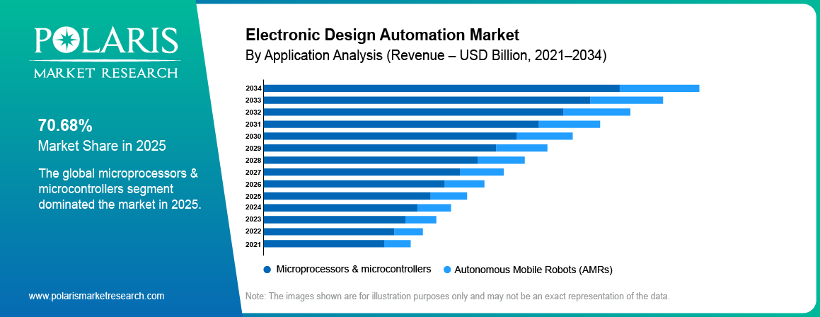
The microprocessors & microcontrollers segment held an 70.68% market share in 2025. The demand for such systems will continue to be influenced by the increasing use of processors in electronic systems. In addition to that, there is increasing development of multi-functional processors within small-sized chips. Such developments increase the demand for software that will help in designing accurate chips. Moreover, the use of such processors in custom-designed systems is also adding to the demand for EDA software. Most of such systems rely on SoC architecture. The segment also overlaps with the ASIC market when there is a demand for product-specific processors. The growing demand for interconnected electronics is also adding to semiconductor design activity.
The memory management units segment is projected to grow at an 10.82% CAGR. The growth in this application segment is driven by the increasing need for memory in modern computing devices. The increasing complexity of processor architecture makes it essential to manage memory efficiently. This increases the design needs in connection with memory-related functions. The EDA software helps to develop these components in the context of broader chip architecture. Another driver for demand includes the rising trend of using SoCs that integrate processing and memory-related functions. The reuse of semiconductor IP (SIP) helps to accelerate the design process of these components by making use of pre-designed memory-related components. With increasing integration of systems, the memory management function is becoming increasingly important in chip architecture.
By End User
The consumer electronics segment accounted for an 29.37% share in 2025. Consumer electronics demand has been driven by the steady development of mobile phones, wearables, computing devices, and interconnected devices. There are constant improvements being made to provide more features while maintaining a small size. This places greater emphasis on chip performance, power consumption, and reliability. EDA tools facilitate the design of chips that are used in all these product categories. In addition, the team involved in the design process can analyze the behavior of products even before manufacturing starts. This can be particularly beneficial where the product life cycle is short, and the design modifications have to be controlled quickly. The increasing use of customized and application-specific chips has increased demand from consumer electronics companies.
The automotive segment is projected to grow at an 11.84% CAGR. Modern automobiles have a high number of electronic components that are utilized for controlling, safety, connectivity, and assistance to drivers. Therefore, there is growing semiconductor usage in vehicles, which leads to increased requirements in regard to automotive chip design. The engineers have to consider various conditions, including heat and signal quality in their design process. Thermal and signal-integrity analysis can support these checks at the design stage. The development of automotive semiconductor technology is highly connected to ISO 26262 standard functional safety requirements. The EDA software allows design teams to meet those requirements during automotive chip development and validation. The higher demand for electronic control systems is leading to increased semiconductor design needs.
EDA vs Manual Chip Design
EDA vs manual design differ mainly in how design tasks are performed and checked. Manual methods can support simple designs, while EDA is better suited to complex semiconductor development.
| Aspect | EDA-Based Design | Manual Chip Design |
| Design speed | The process is automated to carry out similar tasks. | Takes time because it involves more manual work. |
| Accuracy | The software performs checks to detect errors. | Involves more manual work. |
| Design complexity | Has the ability to support larger designs. | More difficult as the design size increases. |
| Verification | Includes specialized tools for testing. | Takes more manual effort to test. |
| Design change | Has the capability of testing after the change. | Necessitates repeated manual efforts. |
| Scalability | Is able to handle advanced semiconductor designs. | Well suited for small designs. |
Source: Polaris Market Research Analysis
Regional Analysis
EDA software regional demand is influenced by the degree of design and fabrication activity in that region. Key markets include North America, Asia Pacific, and Europe. China and India are growing markets for design activity.
North America
The North America electronic design automation market dominated with an 43.86% share in 2025. There is a strong presence of semiconductor and electronics companies in the region. A high proportion of the design work done in the region comes from the U.S. There are efforts from chip developers in the region to develop custom processors as well as other specialized semiconductors. This creates more demand for software that is used at different stages in the development process. There is considerable research and development work in semiconductor engineering as well as electronic systems in the region. Support from the government for the manufacture of domestic semiconductors is stimulating new investments in the industry. Such investments have created further growth prospects for semiconductor design work in the region. Canada is adding to these prospects through increased attention to semiconductor R&D.
Asia Pacific
Asia Pacific led the electronic design automation market is projected to grow at an 11.27% CAGR. Asia Pacific continues to be a vital hub for semiconductor design and manufacturing activities. There is an excellent EDA ecosystem in Taiwan, which is tied to its foundry business. TSMC collaborates with top EDA companies to certify their design tools for its advanced process technologies. Its EDA Alliance also supports design flow across advanced nodes and semiconductor and IC packaging materials. South Korea leverages the design ecosystem of Samsung Foundry as well as its SAFE EDA Alliance. It collaborates with EDA providers to offer certified design flows for its manufacturing processes. Japan is also improving its semiconductor manufacturing abilities through investments in logic manufacturing technology. In April 2026, NEDO approved Rapidus's plans for semiconductor development and chiplet package design at 2 nm (source: rapidus.inc). The initiative also includes PDK availability for customer designs. All these developments help Asia Pacific maintain its leading market share.
China and India: Domestic EDA Push
The ecosystem of semiconductor design in China and India has been evolving due to a renewed emphasis on capabilities within the nation. Both nations have a large number of semiconductor manufacturers and electronics firms that create a need for EDA tools. There are also efforts being made to provide better tooling for chip design and validation. India has been creating its own capabilities in the field of semiconductor design through the sharing of facilities and engineering talent. With an increasing talent pool in semiconductor design, it will be possible for these countries to use their capabilities for both domestic projects and chip designs from across the globe. These countries have also been focusing on building bridges between research institutions and the semiconductor industry. This will result in increased usage of EDA tools in the long run.
Europe
Europe accounted for an 17.42% electronic design automation market share in 2025. There are several semiconductor, automotive, and industrial technology firms in the region. The demand for EDA tools will be driven by the development of chips used for automotive and industrial applications. Moreover, European firms are also investing in advanced semiconductor technology research and production. Germany, France, and the Netherlands are considered key markets for semiconductor designs and related technologies. The governments in the region are financing initiatives aimed at improving the local semiconductor industry. Additionally, the European Chips Act encourages investments in both chip design and production. All these trends create a greater need for design, simulation, and verification software. Growth in advanced electronics is also contributing to the regional EDA market.
Latin America
The Latin America electronic design automation market is projected to grow at an 9.48% CAGR. Demand is rising due to the growing electronics and technology sectors in the region. Brazil and Mexico are among the significant markets because of the existing production capacities. Furthermore, automotive production in the area is driving the demand for advanced electronics systems. This, in turn, drives demand for software that is used for semiconductor and electronics development. In addition, universities and other scientific institutions in the region are contributing to engineering and technology development ll. The greater application of connected devices is providing further opportunities for electronic design activities. Besides, companies are looking for more effective methods of testing electronic products prior to production.
Middle East & Africa
The Middle East & Africa electronic design automation market is anticipated to account for an 9.81% CAGR. This region has been strengthening its electronics and semiconductor sector through technology investment. Countries like Saudi Arabia, the UAE, and Israel have been increasing their involvement in the advancement of electronics and chips. Israel has well-developed semiconductor design and technology businesses. There is also a significant presence of digital infrastructure and technology development in Saudi Arabia and the UAE. These efforts create new opportunities for electronics design. Electronic design is also needed for applications in telecommunications, industry, and automotive sectors.

Competitive Landscape and Key Players
The electronic design automation market is characterized by highly concentrated competition. The top EDA companies 2026 hold a majority of the global market share. Competition has also increased from specialty vendors that serve specific design phases and/or geographic markets. Vendors are working on expanding their portfolio of services to include more phases in the semiconductor design process. Recent mergers have played an important role in increasing capabilities in simulation, SoC design, and design optimization among leading players. Alliances with foundries are also an important aspect of competition. Vendors partner with foundries to validate their tools for process technology and support the customer design flow. Such alliances influence the tool choice, especially for designs at advanced nodes. Foundry certification increases the compatibility of the EDA software with manufacturing needs. Thus, the competitive landscape is driven not only by software capabilities but also by ecosystem relationships.
Vendor Positioning
| Vendor | Core position |
| Aldec | RTL simulation and verification for FPGA and ASIC designs |
| Altium | PCB design and electronics development |
| Ansys | Multiphysics simulation for chips and electronic systems |
| Autodesk | PCB and electronics design through Fusion |
| Blue Pearl Software | RTL analysis and design verification |
| IC design, verification, packaging, PCB, and system design | |
| Intel | Chip design, process technology, packaging, and foundry services |
| Keysight Technologies | RF, high-speed, and electronic system design |
| MathWorks | Model-based design and HDL development for FPGA, ASIC, and SoC |
| PDF Solutions | Semiconductor analytics, yield management, and manufacturing data |
| Siemens EDA | IC verification, PCB design, and 3D IC development |
| Silvaco | TCAD, device modeling, and IC design |
| Chip design, verification, semiconductor IP, and EDA software |
Source: Polaris Market Research Analysis
Buyer Landscape
The main EDA buyers are fabless companies, IDMs, foundries, OEMs, and research institutions. These companies make use of EDA tools for designing and testing electronic products. Semiconductor companies and IDMs are mainly focused on developing new chips. Foundries and OEMs use the tools for production and quality control. Research institutions make use of EDA software for learning and innovation. These users have varying requirements. Hence, EDA solutions are tailored to their needs and the size of their operations.
Recent Developments
- September 2026: Synopsys, Inc. announced new innovations with TSMC. Synopsys stated that the innovations will accelerate the development of next-generation AI and advanced semiconductor systems. Through AI-powered EDA flows and silicon-proven Interface and Foundation IP, the companies are helping customers address growing design complexity. (source: synopsys.com)
- September 2026: IC-Link by imec announced expanded collaboration with TSMC. The collaboration focuses on simplifying customer access to advanced-node semiconductor design capabilities. (source: imec-int.com)
- July 2026: Synopsys, Inc. introduced new autonomous agentic AI workflows for chip design. The company stated that the workflows have been developed in collaboration with Microsoft. They are available for evaluation on Microsoft Discovery. (source: synopsys.com)
Future Outlook
The electronic design automation market is predicted to maintain its significance in view of the increasingly complex nature of chip designs. There will be an increasing demand for such services in the development and application of specific semiconductor chips. Moreover, EDA companies are expected to adopt more innovative approaches and computing architectures, in line with the growing adoption of automation technologies, to meet ever-changing design needs. The industry is projected to witness increased usage not only by existing semiconductor players but also by emerging design houses.
Research Methodology
Overview
The electronic design automation market estimate combines top-down and bottom-up modeling. The base year is 2025, historical data covers 2021–2024, and the forecast runs 2026–2034. Values are in USD billion.
Secondary research
Company annual reports and investor presentations, foundry and industry-body publications, government semiconductor program documents, vendor press releases and conference announcements.
Primary research
Structured interviews with EDA vendor executives, fabless and IDM design leads, and foundry ecosystem managers, used to validate segment shares, pricing models, and adoption trends.
Estimation and triangulation
Vendor revenues are built up by product category, deployment mode, and region, then cross-checked against semiconductor R&D spending and design-start activity. Divergences between sources are reconciled by scope.
Scope and validation
Coverage includes software, semiconductor IP, and services. Forecasts are reviewed by a second analyst and refreshed on a fixed cadence, with the update date reflecting an actual content change.
Electronic Design Automation Market Segmentation
By Product Category Outlook (Revenue, USD Billion, 2021–2034)
- Computer-aided Engineering (CAE)
- Semiconductor Intellectual Property (IP)
- IC Physical Design and Verification
- PCB (Printed Circuit Board) and MCM (Multi-chip Module)
- Services
By Deployment Mode Outlook (Revenue, USD Billion, 2021–2034)
- On-Premises
- Cloud-Based
- Hybrid (Burst to Cloud)
By Workflow Stage Outlook (Revenue, USD Billion, 2021–2034)
- Front-End Design Tools
- Verification Tools
- Physical Design Tools
- Sign-Off Tools
- Packaging & System-Level Tools
By Application Outlook (Revenue, USD Billion, 2021–2034)
- Microprocessors & Microcontrollers
- Memory Management Units
- Others
By End User Outlook (Revenue, USD Billion, 2021–2034)
- Automotive
- Healthcare
- Aerospace & Defense
- Telecom and Data Center
- Consumer Electronics
- Industrial Sector
- Others
By Regional Outlook (Revenue, USD Billion, 2021–2034)
- North America
- US
- Canada
- Europe
- Germany
- France
- UK
- Italy
- Spain
- Netherlands
- Russia
- Rest of Europe
- Asia Pacific
- China
- Japan
- India
- Malaysia
- South Korea
- Indonesia
- Australia
- Vietnam
- Rest of Asia Pacific
- Middle East & Africa
- Saudi Arabia
- UAE
- Israel
- South Africa
- Rest of Middle East & Africa
- Latin America
- Mexico
- Brazil
- Argentina
- Rest of Latin America
Electronic Design Automation Market Report Scope
| Report Attributes | Details |
| Market Size Value in 2025 | USD 18.72 billion |
| Market Size Value in 2026 | USD 20.31 billion |
| EDA Market Forecast 2034 | USD 39.73 billion |
| CAGR | 8.7% from 2026 to 2034 |
| Base Year | 2025 |
| Historical Data | 2021–2024 |
| Forecast Period | 2026–2034 |
| Quantitative Units | Revenue in USD billion and CAGR from 2026 to 2034 |
| Report Coverage | Revenue Forecast, Market Competitive Landscape, Growth Factors, and Industry Trends |
| Segments Covered |
|
| Regional Scope |
|
| Competitive Landscape |
|
| Report Format |
|
| Customization | Report customization as per your requirements with respect to countries, regions, and segmentation. |
Source: Polaris Market Research Analysis
Electronic Design Automation Market FAQ's
The electronic design automation market was valued at USD 18.72 billion in 2025. It is expected to grow to USD 39.73 billion by 2034.
The market is projected to register a CAGR of 8.7% from 2026 to 2034.
Electronic design automation is software that is utilized for designing and testing electronic systems. It is used by engineers to design and test the semiconductor designs prior to the manufacturing process.
In 2025, North America held the largest market share in the global EDA market, at 43.86%. This region possesses a robust ecosystem for the design and manufacturing of semiconductors.
In 2025, on-premises deployment held the largest market share at 58.74%. This is because many organizations want to maintain their design data and software internally.
Key companies include Aldec, Altium, Ansys, Autodesk, Blue Pearl Software, Cadence Design Systems, Intel, Keysight Technologies, MathWorks, PDF Solutions, Siemens EDA, Silvaco, Synopsys, and Zuken.
AI is being added to EDA software for tasks such as design optimization and verification. It is also being used to support RTL development and other design work.
Agentic AI refers to software that can carry out certain chip design tasks with limited human input. Current agentic AI chip design uses include design verification and physical design work.
Chiplets and 3D ICs involve several dies within one system. 3D IC EDA tools help engineers handle the added design and verification requirements.
The high cost associated with licensing can make the software quite expensive to use. Some of the other challenges include a lack of expertise among engineers and lengthy verification processes.
Research firms may include different products, services, and companies in their market calculations. Their data sources and methods can also vary.
Download Sample Report of Electronic Design Automation Market
Please fill out the form to request a customized copy of the research report.


