
Wet Process Equipment Market Demand, Growth Opportunity, 2025-2034
REPORT DETAILS
REPORT DETAILS
ABOUT THIS REPORT
Market Statistics
Overview
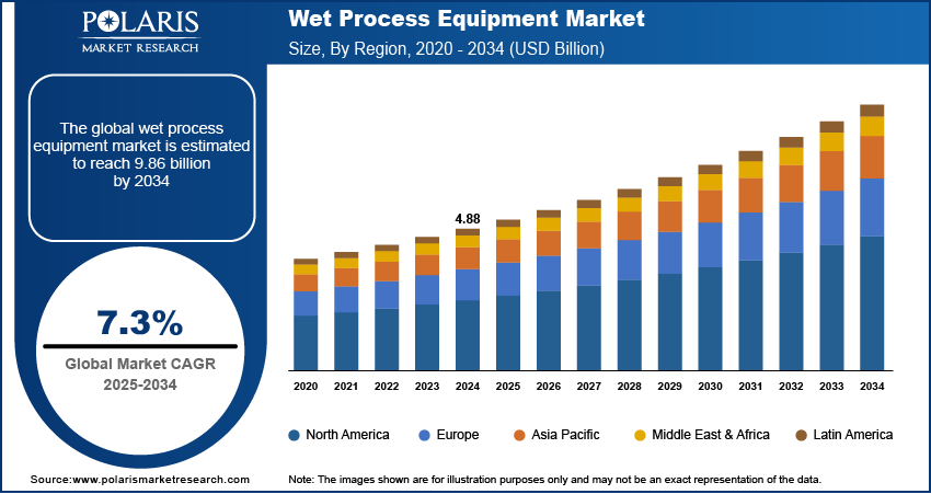
The global wet process equipment market size was valued at USD 4.88 billion in 2024, growing at a CAGR of 7.3% from 2025 to 2034. Increasing demand for miniaturized chips in AI, 5G, and IoT technologies is boosting the need for wet process equipment capable of handling high-precision, low-defect processes at sub-10nm nodes.
Key Insights
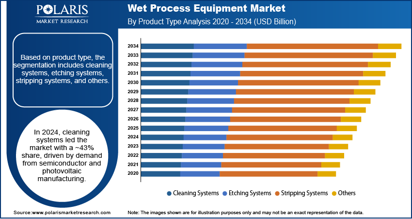
- The cleaning systems segment dominated the market in 2024 with ~43% of the revenue share due to high wafer defect sensitivity in semiconductor and photovoltaic manufacturing.
- The automatic segment held ~57.5% of the revenue share in 2024 as manufacturers in the semiconductor and solar industries are prioritizing throughput, process repeatability, and operator safety.
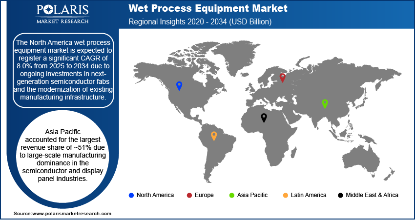
- The North America wet process equipment market is expected to register a significant CAGR of 8.0% from 2025 to 2034 due to ongoing investments in next-generation semiconductor fabs and modernization of existing manufacturing infrastructure.
- The U.S. dominated the North America market due to strong governmental support, high R&D intensity, and the presence of key semiconductor manufacturers.
- Asia Pacific accounted for the largest revenue share of ~51% due to large-scale manufacturing dominance in the semiconductor and display panel industries.
- China led the Asia Pacific market due to aggressive national strategies to reduce dependency on imported semiconductor equipment and boost self-sufficiency in chip manufacturing.
Industry Dynamics
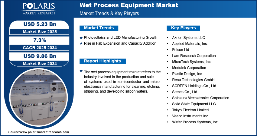
- Growing demand for advanced semiconductors in artificial intelligence (AI), electric vehicles (EVs), and 5G is driving investments in wet process equipment.
- Expansion of semiconductor fabs globally, especially in Asia and the U.S., is boosting demand for high-precision cleaning and etching tools.
- The opportunity lies in developing eco-friendly, water- and chemical-efficient wet processing technologies to meet sustainability and regulatory requirements.
- High capital costs and complex maintenance needs of wet process equipment limit adoption in smaller fabrication facilities.
Market Statistics
- 2024 Market Size: USD 4.88 billion
- 2034 Projected Market Size: USD 9.86 billion
- CAGR (2025–2034): 7.3%
- Asia Pacific: Largest market in 2024
To Understand More About this Research: Download Sample Report
The wet process equipment market refers to the industry involved in the production and sale of systems used in semiconductor and microelectronics manufacturing for cleaning, etching, stripping, and developing silicon wafers. These systems use liquid chemicals to treat wafers during various steps of fabrication, ensuring precision and defect-free processing. Wet process equipment is critical in advanced semiconductor nodes, photovoltaics, micro-electro-mechanical systems (MEMS), LED fabrication, and packaging applications. The market supports both batch and single-wafer processing systems and caters to foundries, integrated device manufacturers (IDMs), and research institutes focused on nanotechnology and electronics. Global investments in semiconductor fabrication plants, especially in Asia and the U.S., are accelerating the need for wet benches and advanced wafer cleaning systems to support new production lines.
Rapid developments in MEMS for automotive, medical, and consumer electronics applications require fine-geometry processing, thereby increasing the demand for high-precision wet process tools. Moreover, growth in heterogeneous integration and advanced packaging technologies such as through-silicon via (TSV) requires reliable wet etching and cleaning solutions, fueling market expansion.
Drivers & Opportunities
Photovoltaics and LED Manufacturing Growth: Surging demand for solar energy and energy-efficient lighting is fueling investments in photovoltaics and LED manufacturing. According to the U.S. Department of Energy, in 2023, solar energy installations in the U.S. reached a record 32.4 gigawatts (GW), marking a 51% increase from 2022, driven by federal incentives under the Inflation Reduction Act. Wet process equipment plays a vital role in these industries for tasks such as wafer texturing, surface cleaning, and passivation, all of which are critical to improving device efficiency and yield. In solar cell production, precision wet processing enhances light absorption and minimizes reflection, directly contributing to improved conversion efficiency. LED fabrication, on the other hand, requires clean and defect-free surfaces to ensure brightness and longevity. Manufacturers are increasingly adopting automated wet benches and single-wafer processing tools to meet throughput demands while maintaining low operating costs.
Rise in Fab Expansion and Capacity Addition: Massive investments are being made in semiconductor fabrication facilities globally, particularly in regions aiming to localize chip production and reduce supply chain risk. The European Commission's 2023 report indicates that over USD 77 billion has been allocated for semiconductor manufacturing investments by EU member states, emphasizing the region's commitment to strengthening its production capabilities. New fabs require advanced wet process equipment to handle delicate wafer surfaces and support high-volume, low-defect manufacturing. From wafer cleaning to oxide etching, wet benches and advanced spin-rinse-dry systems are being deployed across front-end and back-end lines. Foundries and integrated device manufacturers are prioritizing equipment that enables high yields, precision, and chemical use efficiency. This surge in capacity expansion is significantly boosting the sales of wet process tools, especially those compatible with advanced node manufacturing and next-generation packaging technologies.
Segmental Insights
Product Type Analysis
Based on product type, the segmentation includes cleaning systems, etching systems, stripping systems, and others. The cleaning systems segment dominated the market in 2024, with ~43% of the revenue share, as high wafer defect sensitivity in semiconductor and photovoltaic manufacturing has pushed demand for precise and reliable cleaning systems. These tools are crucial in eliminating particulates, metal ions, and organic contaminants before and after critical process steps. Advancements in node scaling and 3D device architectures have increased the frequency and complexity of cleaning cycles, favoring the use of wet bench and single-wafer cleaning systems. Equipment suppliers are focusing on innovations that reduce water and chemical usage while maintaining high cleaning efficiency. Growing integration of AI-driven monitoring and real-time defect tracking in cleaning systems further reinforces their importance in advanced fabs.
The stripping systems segment is expected to register the highest CAGR from 2025 to 2034. Complex multi-layer structures in next-generation chips require more frequent and precise photoresist removal processes, driving the adoption of advanced stripping systems. Increased demand for 3D NAND and FinFET technologies is raising the bar for residue-free and low-damage stripping. Equipment makers are optimizing chemistries and process modules to ensure compatibility with high-aspect-ratio and fragile substrates. Regulatory focus on reducing hazardous waste is also encouraging the development of eco-friendly stripping solutions. These factors are collectively contributing to strong growth prospects for stripping equipment, particularly in fabs transitioning to nodes below 7nm and high-volume packaging applications.
Type Analysis
In terms of type, the segmentation includes automatic, semi-automatic, and manual. The automatic segment held ~57.5% of the revenue share in 2024 as manufacturers in the semiconductor and solar industries are prioritizing throughput, process repeatability, and operator safety. Fully automatic wet process systems offer closed-loop control, reduced manual intervention, and seamless recipe integration, which enhances productivity in high-mix, high-volume settings. Strong return on investment, enabled by reduced contamination risk and minimal operator errors, is making automatic tools a preferred choice in new fab expansions. Continuous improvement in software-driven automation, predictive maintenance, and smart process control is further expanding adoption. Equipment vendors are also offering modular automation solutions tailored to specific wafer sizes and cleanroom footprints.
The semi-automatic segment is expected to register the highest CAGR from 2025 to 2034. Growing interest from small-to-mid-sized fabs and research facilities is driving demand for semi-automatic systems. These tools offer a balance between process control and capital cost, making them suitable for low-volume production and prototyping. Increased R&D activity in MEMS, optoelectronics, and compound semiconductors is creating new use cases where full automation is not feasible or required. Flexibility in handling multiple wafer types and processes on a single platform is another key advantage. Manufacturers are incorporating touch-screen interfaces, recipe customization, and real-time monitoring into semi-automatic systems, aligning them with evolving user expectations without raising operational complexity.
Application Analysis
In terms of application, the segmentation includes semiconductor, MEMS, solar, and others. The semiconductor segment held the largest revenue share of ~78% in 2024 due to aggressive scaling, advanced packaging, and heterogeneous integration in semiconductor manufacturing demand precise and repeatable wet processing steps across etching, cleaning, and surface prep. Foundries and IDMs are investing in state-of-the-art wet benches to meet the requirements of sub-5nm nodes and beyond. Extensive use of wet cleaning at various fabrication stages, including pre-lithography and post-etch, is reinforcing the dominance of this application segment. Increasing demand for logic, memory, and power chips is amplifying fab activity, particularly in front-end-of-line (FEOL) processes where wet process control is critical. Equipment reliability, chemical compatibility, and particle control remain key buying criteria.
The MEMS segment is expected to record the highest CAGR from 2025 to 2034, fueled by the rising adoption of MEMS devices in consumer electronics, automotive sensors, and medical diagnostics. These micro-scale devices require highly customized wet processing steps to ensure uniformity and performance without damaging delicate structures. Increased deployment in wearables, LiDAR, and implantable medical devices is creating complex design needs, where batch and single-wafer wet processes must deliver exceptional repeatability. Equipment designed for MEMS fabrication supports non-standard wafer sizes, custom cleaning cycles, and tight control over film stress and etch rates. This diversity in device architecture and application is supporting robust demand for specialized wet process tools.
Regional Analysis
The North America wet process equipment market is expected to register a significant CAGR of 8.0% from 2025 to 2034 due to ongoing investments in next-generation semiconductor fabs and modernization of existing manufacturing infrastructure. For instance, in June 2025, Texas Instruments announced to allocate over USD 60 billion toward the production of foundational semiconductors within the U.S., aiming to significantly boost domestic manufacturing capabilities and meet the rising demand for advanced semiconductor technologies. The rising focus on domestic chip production, driven by supply chain concerns and policy incentives, is driving demand for advanced wafer cleaning and surface treatment tools. Multiple U.S.-based and global semiconductor companies are initiating new capacity expansion projects, prompting the need for scalable, automated wet process solutions. Emerging trends in 5G infrastructure, AI chipsets, and edge computing applications are further strengthening the demand for high-precision processing equipment. Research institutes and technology developers are also pushing the adoption of MEMS and optoelectronic components, encouraging further innovation in wet benches and etching systems.
U.S. Wet Process Equipment Market Insights
The U.S. dominated the North America market in 2024 due to strong governmental support, high R&D intensity, and presence of key semiconductor manufacturers. Federal initiatives such as the CHIPS and Science Act are offering funding and incentives for domestic semiconductor fabrication and research, directly increasing equipment procurement. The concentration of foundries, universities, and OEMs is fostering a supportive ecosystem for equipment makers and fab operators. Local demand for advanced chips in defense, automotive electronics, and healthcare technologies is fueling investments in cleanroom infrastructure and precision cleaning tools. In the U.S., fabs are increasingly integrating automated and IoT-enabled wet process systems to enhance throughput and yield, supporting continued market growth across advanced node manufacturing.
Asia Pacific Wet Process Equipment Market Trends
Asia Pacific accounted for the largest revenue share of ~51% in 2024, due to large-scale manufacturing dominance in the semiconductor and display panel industries. Countries such as Taiwan, South Korea, China, and Japan host high-volume fabs that require large fleets of wet benches and automated chemical processing tools. Massive capital investments in wafer fabrication and high-density packaging are being driven by consumer electronics, automotive, and data center applications. Equipment procurement in the region is benefiting from shorter supply chains, cost-effective labor, and proximity to leading chip assemblers. Additionally, regional governments are launching subsidy programs to expand domestic semiconductor capacity, ensuring steady long-term demand for wet process equipment across logic, memory, and advanced packaging lines.
China Wet Process Equipment Market Overview
China led the Asia Pacific market in 2024 due to aggressive national strategies to reduce dependency on imported semiconductor equipment and boost self-sufficiency in chip manufacturing. According to the Semiconductor Industry Association, as China produces 36% of global electronics, it plays a central role in semiconductor chip demand and supply. It stands as the second-largest consumer market for chip-embedded electronic devices. Significant state-led funding is supporting the expansion of domestic fabs, elevating demand for front-end process equipment, including wafer cleaning and stripping systems. Several local equipment providers are emerging in the space, and partnerships with global players are helping accelerate technology transfer. Increasing chip design activity and deployment of AI and IoT devices are strengthening demand for smaller node manufacturing, pushing equipment performance standards higher. China’s emphasis on vertical integration across chip design, production, and packaging is creating a holistic environment that supports strong equipment adoption.
Europe Wet Process Equipment Market Outlook
The market in Europe is growing significantly due to a surging focus on strengthening semiconductor sovereignty, driven by regional supply chain vulnerabilities and digital transformation goals. Investments in EU-based fabrication facilities and support through the European Chips Act are enabling capital inflows into semiconductor infrastructure. Key automotive and industrial electronics markets are boosting demand for power chips and sensors, creating opportunities for MEMS and silicon carbide manufacturing, which depend on specialized wet processing tools. Research consortia and government-industry collaborations are fostering innovation in photonic chips and compound semiconductors, expanding the need for advanced, customizable wet benches and cleaning platforms. Environmental regulations are also guiding a shift toward eco-efficient, low-waste wet process solutions across the region.
Key Players and Competitive Analysis
The competitive landscape of the wet process equipment market is defined by continuous innovation, strategic alignment, and strong capital investment across the semiconductor and advanced electronics industries. Industry analysis reveals heightened focus on cleanroom automation, miniaturization, and contamination control, prompting companies to refine product portfolios and scale manufacturing capabilities. Market expansion strategies often involve joint ventures and strategic alliances with regional fabs and material suppliers to ensure faster customization and integration of advanced tools.
Mergers and acquisitions are playing a key role in consolidating technological capabilities, particularly in wafer cleaning, etching, and stripping domains, while post-merger integration is improving supply chain efficiency and product standardization. Technology advancements, especially in IoT-enabled automation, AI-assisted defect detection, and environmentally sustainable processing, are becoming vital differentiators. Players are focusing on modular wet benches, high-throughput batch systems, and multi-process platforms to address varying fab requirements. Cross-industry collaboration and precision manufacturing standards are further intensifying competition, particularly in high-growth applications such as MEMS, compound semiconductors, and photonics.
Key Players
- Akrion Systems LLC
- Applied Materials, Inc.
- Felcon Ltd.
- Lam Research Corporation
- MicroTech Systems, Inc.
- Modutek Corporation
- Plastic Design, Inc.
- Rena Technologies GmbH
- SCREEN Holdings Co., Ltd.
- Semes Co., Ltd.
- Shibaura Mechatronics Corporation
- Solid State Equipment LLC
- Tokyo Electron Limited
- Veeco Instruments Inc.
- Wafer Process Systems, Inc.
Wet Process Equipment Industry Developments
In April 2025, Tokyo Electron Miyagi completed a new development building to support growing semiconductor demand, enhancing capabilities in advanced patterning and etch systems for next-generation chips.
In September 2024, Tokyo Electron Ltd. announced plans to expand in India by hiring and training semiconductor engineers by 2026, supporting India’s push to strengthen domestic chip manufacturing.
April 2025, Veeco Instruments Inc. announced that its WaferStorm and WaferEtch platforms have received global IDM qualification for two new applications in the advanced packaging sector.
November 2024, Veeco Instruments Inc. secured more than USD 50 million in orders for its wet processing systems, which are critical for advancing packaging technologies in artificial intelligence applications.
Wet Process Equipment Market Segmentation
By Product Type Outlook (Revenue, USD Billion, 2020–2034)
- Cleaning Systems
- Etching Systems
- Stripping Systems
- Others
By Type Outlook (Revenue, USD Billion, 2020–2034)
- Automatic
- Semi-automatic
- Manual
By Application Outlook (Revenue, USD Billion, 2020–2034)
- Semiconductor
- MEMS
- Solar
- Others
By Regional Outlook (Revenue, USD Billion, 2020–2034)
- North America
- U.S.
- Canada
- Europe
- Germany
- France
- UK
- Italy
- Spain
- Netherlands
- Russia
- Rest of Europe
- Asia Pacific
- China
- Japan
- India
- Malaysia
- South Korea
- Indonesia
- Australia
- Vietnam
- Rest of Asia Pacific
- Middle East & Africa
- Saudi Arabia
- UAE
- Israel
- South Africa
- Rest of Middle East & Africa
- Latin America
- Mexico
- Brazil
- Argentina
- Rest of Latin America
Wet Process Equipment Market Report Scope
| Report Attributes | Details |
| Market Size in 2024 | USD 4.88 billion |
| Market Size in 2025 | USD 5.23 billion |
| Revenue Forecast by 2034 | USD 9.86 billion |
| CAGR | 7.3% from 2025 to 2034 |
| Base Year | 2024 |
| Historical Data | 2020–2023 |
| Forecast Period | 2025–2034 |
| Quantitative Units | Revenue in USD billion and CAGR from 2025 to 2034 |
| Report Coverage | Revenue Forecast, Competitive Landscape, Growth Factors, and Industry Trends |
| Segments Covered |
|
| Regional Scope |
|
| Competitive Landscape |
|
| Report Format |
|
| Customization | Report customization as per your requirements with respect to countries, regions, and segmentation. |
FAQ's
The global market size was valued at USD 4.88 billion in 2024 and is projected to grow to USD 9.86 billion by 2034.
The global market is projected to register a CAGR of 7.3% during the forecast period.
Asia Pacific accounted for the largest revenue share of ~51% due to large-scale manufacturing dominance in the semiconductor and display panel industries.
A few of the key players in the market are Akrion Systems LLC; Applied Materials, Inc.; Felcon Ltd.; Lam Research Corporation; MicroTech Systems, Inc.; Modutek Corporation; Plastic Design, Inc.; Rena Technologies GmbH; SCREEN Holdings Co., Ltd.; Semes Co., Ltd.; Shibaura Mechatronics Corporation; Solid State Equipment LLC; Tokyo Electron Limited; Veeco Instruments Inc.; and Wafer Process Systems, Inc.
The cleaning systems segment dominated the market with ~43% of the revenue share in 2024, as high wafer defect sensitivity in semiconductor and photovoltaic manufacturing has pushed demand for precise and reliable cleaning systems.
The automatic segment held ~57.5% of the revenue share in 2024 due to manufacturers in the semiconductor and solar industries are prioritizing throughput, process repeatability, and operator safety.
Download Sample Report of Wet Process Equipment Market
Please fill out the form to request a customized copy of the research report.
