
Advanced IC Substrates Market Size, Share, Trends & Forecast, 2026–2034
REPORT DETAILS
Advanced IC Substrates Market Summary
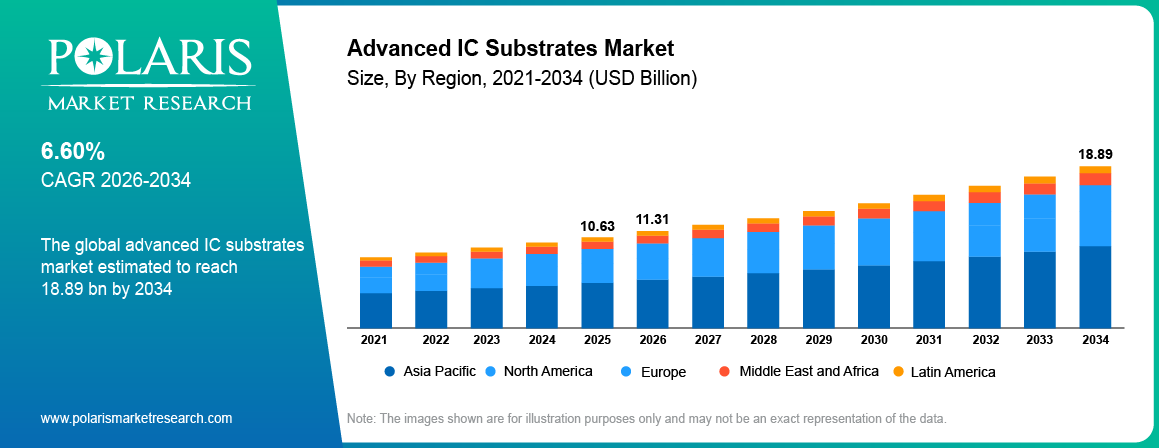
The advanced IC substrates market size was valued at USD 10.63 billion in 2025. Market is projected to register a CAGR of 6.60% during 2026–2034. Rising demand for AI accelerators, high-performance computing, and enhanced semiconductor packaging drives the market growth. Also, increasing requirements for automotive electronics and high-density electronic devices fuel market growth.
Market Statistics
Advanced IC Substrates Market Key Takeaways
- Asia Pacific dominated the global advanced IC substrates market share with 65.73% in 2025. The dominance is attributed to its strong semiconductor and electronic ecosystem.
- The North America advanced IC substrates market is expected to register the highest
- CAGR of 9.67% during the forecast period. The growth is fueled by increasing adoption of advanced electronics.
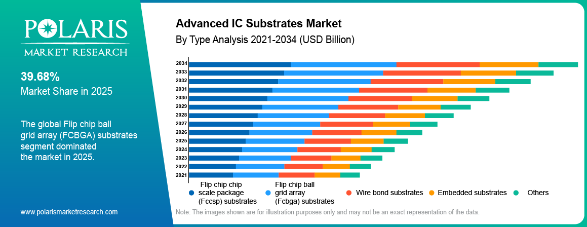
- The FCBGA substrates segment held the largest share of 39.68% in 2025. It is driven by the expansion of AI, HPC, servers, and networks.
- The HDI substrates segment accounted for a significant share of 34.86% in 2025. The dominance is fueled by downsizing and high-density routing.
- The mobile and consumer electronics segment held a 35.74% market share in 2025. The leading share is supported by increasing emphasis on miniaturization and high volumes of devices.
Note: Figures and projections outlined in this report are the result of Polaris Market Research’s proprietary analytical processes, grounded in the latest available datasets and market observations.
What is an Advanced IC Substrate?
Advanced IC substrates are specialized baseboards used to package bare integrated circuit chips. They provide essential functions such as structural support, electrical connections, and heat management for high-performance electronic devices. They are a critical link between the IC chip and the printed circuit board. Advanced IC substrates enable advanced features and miniaturization.
Advanced semiconductor substrates are used in smartphones, computer components, data centers, networking systems, automotive electronics, artificial intelligence (AI) systems and other high-performance electronic goods. The increasing semiconductor integration and the complexity of packages are pushing the demand for substrates with finer circuits and a greater number of layers. The advanced IC substrates market forecast 2034 reflects continued demand from AI, HPC, advanced packaging, automotive electronics, and high-density consumer devices.
How Advanced IC Substrates Work
Advanced IC substrates are the interconnect between the semiconductor package and the main circuit board. They help transfer power and information, provide mechanical support to the chip, and regulate heat created during operations.
Standard procedure includes:
- Materials Preparation: Prepare substrate core, dielectrics, and copper layers.
- Circuit Design: Design circuits in a complex way using advanced methods.
- Layer Build-Up: Increase routing capacity by adding more dielectric and copper layers.
- Drilling & Metallization: Generate microvias and define inter-layer connections.
- Surface Preparation: Prepare the surface of the substrate for attaching the semiconductor.
- Inspection: Electrical performance, size, warpage, and manufacturing quality.
- Package Integration: Integrate the substrate with the semiconductor package and system board.
Traditional Packaging vs Advanced IC Substrates
| Attribute | Traditional Packaging | Advanced IC Substrates |
| Performance | Standard chip-to-board connection | High-speed signal performance tuned for AI/HPC workloads |
| Density | Lower interconnect capability | Higher circuit density via finer lines and smaller vias |
| Core material options | Single conventional laminate | ABF, BT resin, glass, and ceramic cores by application |
| Applications | Basic consumer electronics | AI accelerators, HPC, automotive electronics, advanced processors |
| Thermal management | Limited | Improved heat handling for high-power dies |
| Manufacturing complexity | Lower | Advanced manufacturing (SAP/mSAP, laser drilling, panel-level processing) |
Source: Polaris Market Research Analysis
The increasing adoption of Internet of Things (IoT) devices across various sectors, from smart homes and wearables to industrial automation and healthcare, is significantly boosting the demand for advanced IC substrates. These devices often require highly integrated, compact, and energy-efficient electronic components, which advanced IC substrates are designed to enable. As the IoT ecosystem expands, there is a rising need for specialized substrates that support reliable connectivity, efficient data processing, and miniaturization in these smart devices.
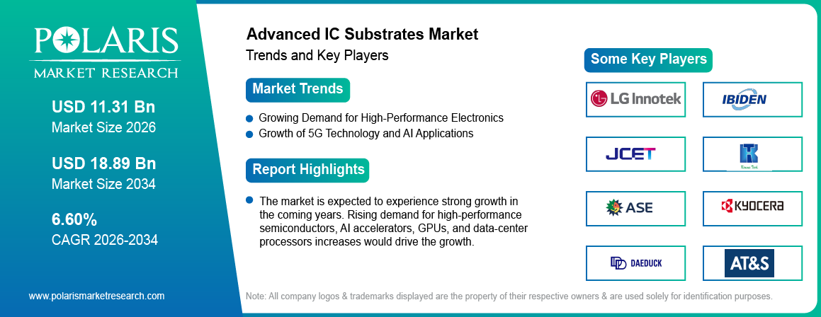
Continuous innovation in semiconductor packaging, such as heterogeneous integration and chiplet-based architectures, is a major driver for the advanced IC substrates market. These advanced packaging methods enable the integration of multiple distinct chips or functionalities into a single package, leading to improved performance, reduced power consumption, and smaller form factors. This evolution in packaging directly drives the need for more sophisticated and high-density IC substrates that can facilitate the complex interconnections and thermal management required by these next-generation integrated circuits.
Market Dynamics
Driver: Growing Demand for High-Performance Electronics
The increasing use of high performance electronics across computing, consumer electronics, automotive, and industrial applications is driving the advanced IC substrates market growth. There is a rising need for electronic devices that can handle more complex tasks and process data faster. Modern electronics such as powerful smartphones, advanced gaming consoles, and sophisticated automotive systems require substrates that can support higher circuit densities, better signal integrity, and improved thermal management. These high-performance requirements push manufacturers to develop more advanced and efficient substrate solutions.
The rising adoption of various digital health technologies, including wearable devices and remote monitoring systems, highlights the increasing demand for high-performance electronics in the healthcare sector. Also, the adoption of electric vehicles (EVs) is growing across the world. BloombergNEF expects 23.3 million passenger EVs to be sold worldwide in 2026, up 11% year-on-year, largely driven by China. The need for substrates with efficient electrical routing, signal integrity, and thermal performance is being driven by higher processing requirements and greater component density. The increasing demand for high-performance processors, servers, and networking equipment further supports the growing market of FC-BGA substrates (Source: bnef.com).
Driver: Growth of 5G Technology and AI Applications
The widespread rollout of 5G networks and the rapid expansion of artificial intelligence (AI) applications are fueling a substantial demand for advanced IC substrates. According to 5G Americas, 5G connections reached 2.25 billion in 2024 and are forecast to reach 8.3 billion globally by 2029. 5G devices require advanced substrates with higher I/O density, faster signal transmission and better thermal management. Therefore, the expansion of 5G networks is driving demand for advanced substrate solutions. (Source: 5gamericas.org)
The proliferation of AI in various sectors, including medical devices, necessitates advanced electronic components capable of handling complex algorithms and massive datasets. AI require processors and supporting components that can manage incredibly high data rates, low latency, and significant computational power. This puts immense pressure on the packaging technology, making advanced IC substrates crucial for maintaining performance and reliability. The ongoing development and deployment of 5G and AI are, therefore major forces driving the advanced IC substrates market demand.
Driver: Increasing Adoption of Advanced Semiconductor Packaging
The increasing adoption of chiplets, heterogeneous integration, 2.5D packaging, 3D ICs and other advanced packaging technologies is fueling the demand for high-density substrates. These architectures demand substrates that can accommodate complex interconnects and high-speed communication between multiple chips. The growing use of chiplet packaging is generating further demand for substrates for multi-die integration and high-density interconnects.
Driver: Expansion of ABF and Glass-Substrate Capacity
The increasing demand for AI, HPC, and larger semiconductor packages is driving investments in ABF substrate capacity and new glass-core technologies. These developments are enhancing substrate capabilities for high-density packages and creating new opportunities for advanced IC substrate manufacturers. Increasing industry focus on larger package sizes and improved dimensional stability is further driving interest in glass-based substrate technologies.
Restraint: High costs of manufacture and capacity requirements
The manufacturing of an advanced IC substrate requires a large financial investment, complex technology, sophisticated materials, and tight process control. The manufacturing and qualification procedure of a high-end substrate is also complicated. It adversely affects the capacity expansion and production cost.
Opportunity: Glass-Core Substrate Expansion
The increasing size of semiconductor packages is opening up new opportunities with glass core substrates. Glass offers good dimensional stability and can help control warpage in big semiconductor packages. AI and high-speed computing are adopting glass-based technologies at an increasing pace. In September 2026, Samsung Electro-Mechanics exhibited 2.5D, 2.1D and glass substrate solutions for high density semiconductor packaging for AI accelerators and servers (Source: samsungsem.com).
Challenge: Technology and Supply Chain Constraints
The industry has challenges in advanced materials, manufacturing yield, equipment capacity, qualification requirements and concentrated supply chains. Demand for ABF substrates used in AI and HPC is also creating production capacity difficulties.
Tariff and Trade Policy Impact on Advanced IC Substrates
U.S. trade policy is boosting the push for localization of the semiconductor supply chain. In January 2026, the U.S. levied a 25% Section 232 tax on some advanced computer chips and related products, effective January 15, with exemptions for use in U.S. data centers, R&D, startups, and consumer and governmental purposes (Source: whitehouse.gov).
Advanced IC substrates tariff impact may lead to local sourcing, expanded capacity, and supplier diversification for sophisticated IC substrates, notably for advanced packaging and artificial intelligence. The impact will be driven by what specific goods are considered and utilized. The growth in semiconductor localization can stimulate the demand for local packaging and substrate capacity.
Europe announced the enactment of the Chips Act 2.0 in June 2026 that aims to grow semiconductor manufacturing, cut dependency on foreign supply chains, and increase Europe’s technology resilience amidst growing demand for AI-based computing. Together, the U.S. and EU actions are projected to encourage investment in localized semiconductor and advanced packaging ecosystems.
Segmentation Analysis
Advanced IC Substrates Market Segmentation by Type, Technology, Core Material, Packaging Technology, Application and Region
By Type Analysis
Based on type, the segmentation includes flip chip ball grid array (FCBGA) substrates, flip chip chip scale package (FCCSP) substrates, wire bond substrates, embedded substrates, and others. The FCBGA substrates segment captured a significant market share of 39.68% in 2025. The dominance is propelled by its extensive application in central processing units (CPUs), graphics processing units (GPUs), networking devices, AI accelerators, and other high-performance devices. These substrates are widely used in applications that demand high performance and complex chip designs. FCBGA substrates offer excellent electrical performance, superior thermal dissipation, and high-density interconnects. These features are crucial for today's powerful computing and communication systems, driving the FC-BGA substrates market growth. Their ability to manage a large number of input/output (I/O) connections in a compact form factor makes them indispensable for devices requiring significant processing power and data throughput. FCBGA substrates provide better electrical performance and effective heat dissipation.
The Flip Chip Chip Scale Package (FCCSP) substrates segment is anticipated to register the highest CAGR of 8.93% during the forecast period. This growth is driven by the increasing demand for smaller, lighter, and more power-efficient electronic devices, especially in the mobile and wearable technology sectors. FCCSP substrates are small in size but do not compromise on electrical and thermal performance. These features make them ideal for highly miniaturized products where space is at a premium. Thus, their demand is high in used in smartphones, wearables, IoT devices, and other portable electronics. The continued miniaturization of consumer electronic devices is expected to support segment expansion.
Substrate Type Comparison (FC-BGA vs FC-CSP Substrate vs Wire Bond/Embedded Substrates vs Glass Core Substrates)
| Substrate type | Best fit for | Relative cost | Key trade-off |
| FC-BGA | CPUs, GPUs, networking, AI accelerators | Higher | Best I/O density and thermal performance; highest capital intensity to manufacture |
| FC-CSP | Smartphones, ultra-thin consumer devices | Moderate | Smallest footprint; less I/O headroom than FC-BGA |
| Wire bond / embedded substrates | Cost-sensitive, lower-complexity devices | Lower | Simplest to manufacture; limited density and speed |
| Glass core substrates | Sub-4 nm logic, co-packaged optics | Highest (emerging) | Best flatness and optical routing; still scaling production yield |
Source: Polaris Market Research Analysis
By Technology Analysis
Based on technology, the segmentation includes high-density interconnect (HDI) substrates, build-up substrates, coreless substrates, organic substrates, and ceramic substrates. The high-density interconnect (HDI) substrates segment held the largest share of 34.86% in 2025, due to the rising need for compact and highly integrated electronic components. HDI technology accommodates fine lines, small vias, and dense routing required for smartphones, communication devices, and other advanced electronics. These substrates are foundational for modern electronic devices that require compact designs and high levels of integration, such as smartphones, tablets, and wearable technologies. HDI substrates enable the creation of smaller and thinner devices by allowing for finer lines, smaller vias, and increased routing density compared to traditional printed circuit boards. Their widespread adoption is driven by the continuous consumer demand for increasingly sophisticated and miniaturized electronics, where efficient space utilization and enhanced electrical performance are paramount.
The build-up substrates segment is anticipated to register the highest CAGR of 9.71% during the forecast period. This growth is significantly fueled by the increasing complexity of semiconductor packaging, particularly for high-performance computing (HPC), artificial intelligence (AI) applications, and advanced packaging techniques such as chiplets. Build-Up substrates, often incorporating Ajinomoto Build-Up Film (ABF) or similar materials. It allows for multiple layers of circuitry to be constructed sequentially. This offers superior electrical performance, improved signal integrity, and better thermal management capabilities for highly integrated circuits. As processors become more powerful and sophisticated, requiring even finer line widths and greater interconnect density, build-up technology provides the necessary foundation. Build-up substrates are suitable for increasingly complex semiconductor packages since they support multiple circuit layers and fine connections needed for high-speed processors.
By Core Material Analysis
The ABF segment is projected to register the largest share of 51.64% in 2025. Ajinomoto build-up film substrates are a wide range of materials. They are used for the manufacturing of high-performance IC package substrates. ABF material is enabling fine-line circuits and multi-layer architectures. All these benefits boost the segment growth.
The glass segment is expected to record a significant CAGR of 11.27% during the forecast period. The segment observes the quick expansion owing to the development of substrates for high-performance, large-size packages. Glass is rigid and dimensionally stable and is now being studied for future-generation AI and advanced packaging applications.
By Packaging Technology Analysis
The 2D Flip-Chip segment held the largest share of 39.67% in 2025. The dominance is driven by expanded production infrastructure and rising use in CPUs, communications and consumer devices. In this segment, solder bumps directly connect a semiconductor die to a package substrate. The architecture offers short interconnect paths and high I/O density. It also provides improved electrical performance than conventional wire bonding. 2D flip-chips are widely used in CPUs, GPUs, FPGAs, ASICs, and other high-performance devices. Rising demand for AI, HPC, data centers, and high-performance computing propels the need for fine-line, multilayer substrates.
The 2.5D/3D packaging segment is predicted to exhibit a CAGR of 10.36% during the forecast period. The growth is attributed to increased usage of chiplets, HBM and heterogenous integration. It requires high-density interconnects of numerous die/package components.
By Application Analysis
Based on application, the segmentation includes mobile & consumer electronics, automotive electronics, networking & communication devices, computing & data centers, and others. The mobile & consumer electronics segment dominated with 35.74% revenue share in 2025. This dominance is driven by the sheer volume of products in this category, including smartphones, tablets, laptops, and various wearable devices. These electronics are constantly evolving, with consumers demanding thinner, lighter, and more powerful gadgets. This continuous innovation directly translates into a high demand for advanced IC substrates that can accommodate increasingly complex and miniaturized chip designs while ensuring optimal performance and thermal management.
The computing & data centers segment is anticipated to exhibit a substantial CAGR of 11.16% during the forecast period. The growth will be attributed to the increasing demand for substrates used in AI accelerators, server CPUs, and high-performance computing systems. The rising investment in AI accelerator packaging and data-center substrates is pushing substrate manufacturers to increase capacity and create solutions for high-performance server applications.
Advanced IC Substrates Market Regional Insights
Asia Pacific Advanced IC Substrates Market
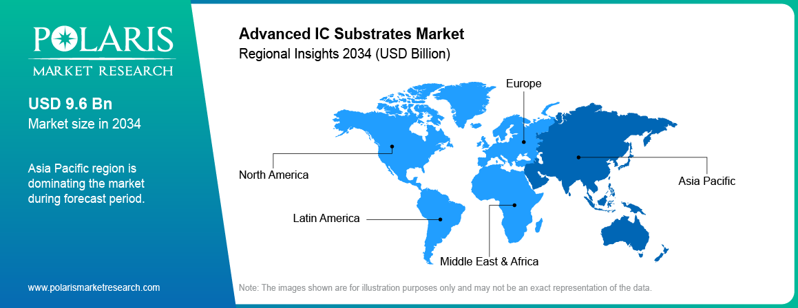
Asia Pacific dominated the global advanced IC substrates market share by holding 65.73% in 2025. The leading position is attributed to its well-established semiconductor manufacturing, packaging, electronics, and substrate manufacturing ecosystem. The region serves as a major hub for the design and manufacturing of a vast array of electronic devices, from smartphones and laptops to complex networking equipment. This high volume of production naturally translates into immense demand for advanced IC substrates, making Asia Pacific a leading region in terms of both consumption and supply. Continuous technological advancements and a large skilled workforce further solidify the region's strong position in the market. China, Japan, South Korea, Taiwan and other regional markets have strong capabilities in package substrates, semiconductor assembly, materials and advanced packaging.
China Advanced IC Substrates Market Overview
China led the Asia Pacific market with 31.67% share in 2026. The country's massive consumer electronics sector and its growing investments in domestics semiconductor capabilities fuel a substantial demand for advanced IC substrates. China's rapid technological progress in areas such as 5G infrastructure and artificial intelligence applications also contributes significantly to the need for high-performance and high-density IC substrates. The ongoing expansion of manufacturing facilities and the increasing focus on advanced packaging technologies within China are key factors propelling the demand for advanced IC substrates.
North America Advanced IC Substrate Market
North America is expected to witness a significant CAGR of 9.67% during the forecast period. It is driven by investments in semiconductor manufacturing, advanced packaging, AI, and data centers. The US policy environment is also encouraging greater localization of semiconductor supply chains. In July 2026, TSMC announced an additional USD 100 billion investment in the U.S., bringing its planned U.S. investment to USD 165 billion according to NIST (Source: nist.gov).
The 2026 Section 232 duty on certain advanced computing chips and broader trade-policy measures could influence sourcing and localization decisions. Semiconductor policy incentives are also supporting advanced packaging investments, including Amkor's planned advanced packaging and test facility in Arizona.
The market growth is also driven by the region’s robust semiconductor innovation ecosystem and increasing adoption of advanced electronics. The region is home to numerous leading technology companies that are at the forefront of developing high-performance computing, AI, and networking solutions. This creates a strong demand for advanced IC substrates that can support advanced chip designs and packaging technologies. Furthermore, the growing focus on domestic manufacturing and supply chain resilience in the semiconductor sector in North America is providing additional momentum for the advanced IC substrates market.
U.S. Advanced IC Substrates Market Insight
In North America, the U.S. dominated with 69.45% in 2025. This is driven by semiconductor research, AI development, computing, and data-center investments. Demand is concentrated in applications requiring high-performance processors and advanced packaging. Government initiatives aimed at strengthening domestic semiconductor production are further supporting investment across the broader semiconductor ecosystem. The presence of major technology firms and ongoing government initiatives aimed at boosting domestic semiconductor production further contribute to the adoption of the advanced IC substrates in the U.S.
Europe Advanced IC Substrates Market in Europe
The market in Europe will exhibit a CAGR of 8.83% during the forecast period, due to the existence of industries such as the automotive, industrial, telecommunication and semiconductor industries. Registrations of new cars in the EU increased by 5.7% in H1 2026, with battery electric cars accounting for 20.7% of the market, compared to 15.6% in H1 2025. Germany and other key European markets are attempting to strengthen resilience in the semiconductor industry (Source: acea.auto).
The EU Chips Act 2.0 proposal aims to enhance the advanced chip manufacturing, reduce strategic dependencies, promote demand-side measures and secure the semiconductor value chain including packaging.
The increasing complexity of electronic systems in modern vehicles, including electric vehicles and advanced driver-assistance systems, drives a significant demand for reliable and high-performance IC substrates. Additionally, Europe's focus on industrial automation and the growing adoption of IoT in manufacturing processes contribute to the need for advanced packaging solutions.
Germany Advanced IC Substrates Market
Germany dominated the European market with 28.43% share in 2025. The dominance is driven by its strong automotive industry. Rising adoption of electric vehicles and autonomous driving technologies propel the need for advanced IC substrates. German manufacturers are among the most advanced electronic systems in vehicles and need high density interconnects and reliable packaging. Furthermore, Germany's strong industrial base and its investments in research and development in microelectronics play a crucial role in driving the market in the region.
Latin America Advanced IC Substrate Market
The market in Latin America is expected to register a 8.17% CAGR during the projected period. The region has electronics manufacturing, automotive manufacturing, and supply chain diversification. Mexico is a key market given its proximity to the U.S. manufacturing ecosystem, while Brazil has prospects in automotive and industrial electronics.
Middle East & Africa Advanced IC Substrates Market
The Middle East & Africa market will record a CAGR of 7.74% during the forecast period. Data-center development, digital infrastructure, telecommunications and electronics upgrading boost the regional market expansion. Demand is still centered on communication infrastructure, computers, and industrial applications.
Use Cases / Real-World Applications
- AI Processor Packaging: High-I/O AI accelerator and processor packaging.
- HPC Platforms: High-performance CPU / GPU / Computing Package.
- Data Centers: Server processors, network chipsets & acceleration platforms.
- Smart Phones & Wearable Devices: Compact, high-density semiconductor packages.
- Automotive Electronics: Infotainment, ADAS/Autonomous Driving, Vehicle Compute.
- 5G Equipment: Devices for high-frequency, high-density communication.
- Gaming: High-performance processor and graphics platform.
- IoT Devices: Integrated, compact semiconductor solution.
Innovation Trends
-
Ultra-thin, coreless substrates
Some new technologies like thinner and coreless substrates are being worked on to make the packages thinner and have high-density circuits. This technology is of great use in mobile and computing applications.
-
AI-Accelerator Packaging
AI accelerators need bigger substrates, more layers, finer circuits, greater I/O density, and better warpage management. Samsung Electro-Mechanics is showing off 2.5D and 2.1D technology for AI and server applications.
-
Chiplet and Heterogeneous Packaging
The need for increasingly sophisticated connection and substrate technologies to integrate several dies and memories into one package is driven by chiplet designs.
-
Glass-Core Substrates
Glass is developing as a next-generation core material due to its dimensional stability and potential benefits for large-area, high-density packaging. Development and ecosystem activities surrounding glass-core technology are ramping up.
-
High-Frequency 5G Materials
The arrival of 5G and high-speed communications is prompting the usage of materials and substrate structures that can handle high-frequency signal transmission with less signal loss.
Competitive Landscape
The advanced IC substrates market consists of current substrate manufacturers, semiconductor packaging firms and electronics technology providers. These players are crucial to its competitive landscape. Competition is increasingly centered on fine-line processing, high-layer-count substrates, ABF capacity, big package sizes, glass-core technologies and innovative packaging capabilities. The competitive environment is also characterized by intense focus on innovation, driven by the escalating demands for higher performance, greater miniaturization, and improved integration in electronic devices. Companies are heavily investing in research and development to create more advanced materials and manufacturing processes, especially to cater to the growing needs of applications such as AI, 5G, and high-performance computing.
Advances in AI and HPC have also encouraged companies to expand capacity near strategic consumers for semiconductors and technologies. The increased focus on high-performance IC substrates for AI and server applications is demonstrated by the recent expansions of AT&S and Ibiden.
List of Advanced IC Substrates Market Key Players 2026
- ASE Technology Holding Co., Ltd. (ASE Group)
- AT&S Austria Technologie & Systemtechnik AG
- Daeduck Electronics Co., Ltd.
- Ibiden Co., Ltd.
- JCET Group Co., Ltd.
- Kinsus Interconnect Technology Corp.
- Kyocera Corporation
- LG Innotek Co., Ltd.
- Nan Ya Printed Circuit Board Corporation
- Samsung Electro-Mechanics Co., Ltd.
- Shennan Circuit Company Limited
- Shinko Electric Industries Co., Ltd.
- SIMMTECH Co., Ltd.
- Toppan Inc.
- TTM Technologies, Inc.
- Unimicron Technology Corporation
Vendor Positioning
| Vendor | Core material strength | Notable 2025–2026 capacity move | Primary end-use focus |
| Ibiden Co., Ltd. | ABF build-up | Ohno Plant (Japan) capacity expansion for AI/server substrates | AI/HPC, servers |
| Unimicron Technology Corp. | ABF, glass (via Corning stake) | Stake in glass pilot line for next-gen core material | AI/HPC, mobile |
| AT&S Austria Technologie & Systemtechnik AG | ABF, high-layer-count FC-BGA | Kulim, Malaysia expansion tied to AMD-linked demand | AI/HPC, automotive |
| Shinko Electric Industries Co., Ltd. | ABF build-up | Recognized as an Intel 2025 supplier award recipient | AI/HPC, computing |
| Samsung Electro-Mechanics Co., Ltd. | ABF build-up | ABF capacity expansion across South Korea and Vietnam | Mobile, AI/HPC |
| ASE Technology Holding Co., Ltd. | Advanced packaging / OSAT integration | New U.S. advanced-packaging capacity investment | AI/HPC, diversified |
Source: Polaris Market Research Analysis
Recent Developments
- In June 2026, The Qnity Advanced Packaging Innovation Hub has been inaugurated, showcasing materials and processes used in the fabrication of advanced IC substrates, interposers, HBM, and high-density interconnects for AI and HPC applications. (Source: qnityelectronics.com)
- In July 2026, ATS announced the expansion of Kulim, Malaysia facility to expand capacity in the area of advanced IC substrate and semiconductor packaging solutions to cater to long-term demand and technology partnerships. (Source: ats.net)
- In May 2026, ASE announced the adoption of automated 310 mm panel-level packaging technology to support next-generation AI and HPC technology requirements. (Source: aseglobal.com)
Future Outlook
The market is expected to experience strong growth in the coming years. Rising demand for high-performance semiconductors, AI accelerators, GPUs, and data-center processors increases would drive the growth. The expansion of advanced packaging technologies, such as 2.5D and 3D integration, chiplets, and high-bandwidth memory, would support demand for high-density substrates with improved electrical and thermal performance. Increasing investments in semiconductor manufacturing and packaging capacity across APAC, North America, and Europe will boost market expansion. Technological advancements in fine-line fabrication, multilayer substrates, and materials would create lucrative market opportunities in the coming years.
Advanced IC Substrates Market Segmentation
By Type Outlook (Revenue, USD Billion, 2021–2034)
- Flip Chip Ball Grid Array (FCBGA) Substrates
- Flip Chip Chip Scale Package (FCCSP) Substrates
- Wire Bond Substrates
- Embedded Substrates
- Others
By Technology Outlook (Revenue, USD Billion, 2021–2034)
- High-Density Interconnect (HDI) Substrates
- Build-Up Substrates
- Coreless Substrates
- Organic Substrates
- Ceramic Substrates
By Core Material Outlook (Revenue, USD Billion, 2021–2034)
- ABF
- BT Resin
- Glass
- Ceramic
- Others
By Packaging Technology Outlook (Revenue, USD Billion, 2021–2034)
- 2D Flip-Chip
- 2.5D Interposer
- 3D-IC / SoIC
- Fan-Out Wafer-Level Packaging (FOWLP)
- SiP / Module
By Application Outlook (Revenue, USD Billion, 2021–2034)
- Mobile & Consumer Electronics
- Automotive Electronics
- Networking & Communication Devices
- Computing & Data Centers
- Others
By Regional Outlook (Revenue, USD Billion, 2021–2034)
- North America
- U.S.
- Canada
- Europe
- Germany
- France
- UK
- Italy
- Spain
- Netherlands
- Russia
- Rest of Europe
- Asia Pacific
- China
- Japan
- India
- Malaysia
- South Korea
- Indonesia
- Australia
- Vietnam
- Rest of Asia Pacific
- Middle East & Africa
- Saudi Arabia
- UAE
- Israel
- South Africa
- Rest of Middle East & Africa
- Latin America
- Mexico
- Brazil
- Argentina
- Rest of Latin America
Advanced IC Substrates Market Report Scope
| Report Attributes | Details |
| Market Size in 2025 | USD 10.63 Billion |
| Market Size in 2026 | USD 11.31 Billion |
| Revenue Forecast by 2034 | USD 18.89 Billion |
| CAGR | 6.60% from 2026 to 2034 |
| Base Year | 2025 |
| Historical Data | 2021–2024 |
| Forecast Period | 2026–2034 |
| Quantitative Units | Revenue in USD Billion and CAGR from 2026 to 2034 |
| Report Coverage | Revenue Forecast, Competitive Landscape, Growth Factors, and Industry Trends |
| Segments Covered |
|
| Regional Scope |
|
| Competitive Landscape |
|
| Report Format |
|
| Customization | Report customization as per your requirements with respect to countries, regions, and segmentation. |
Source: Polaris Market Research Analysis
Advanced IC Substrates Market FAQ's
Advances in IC substrates are the interconnecting elements between semiconductor chips and printed circuit boards providing electrical, mechanical and thermal
In 2025, the market was valued at USD 10.63 billion and is anticipated to reach USD 18.89 billion by 2034, due to rising demand for high-performance electronics.
The market is estimated to develop at a CAGR of 6.60% during the forecast period 2026-2034, increasing adoption of the Internet of Things.
Some of the main driving factors that drive this market include artificial intelligence and HPC applications, developments in packaging methods, chiplets, automotive electronics and high-performance applications.
The FCBGA substrates segment held the largest share of 39.68% in 2025., due to its rising application in CPUs, graphics processing units GPUs, networking devices, AI accelerators, and other high-performance devices
Challenges for this market include high cost, complex production, restricted capacity, limited raw material availability, limited yields and long qualification procedures.
Asia Pacific dominated the global advanced IC substrates market share with 65.73% in 2025 due to its ecosystem connected to semiconductors, electronics, and packaging.
Key technologies in use are AI packaging, ABF build-up, chiplets, 2.5D/3D packaging, glass core substrates, and HDI and panel-level packaging.
Key trends include rising 5G and AI adoption, growing IoT device demand, advancing chiplet and heterogeneous integration packaging, increasing miniaturization needs, and expanding automotive electronics applications globally.
Download Sample Report of Advanced IC Substrates Market
Please fill out the form to request a customized copy of the research report.


