
Atomic Force Microscopy Market Growth Trends, Industry Drivers, 2026-2034
REPORT DETAILS
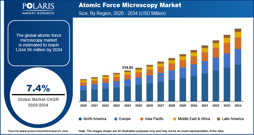
Atomic Force Microscopy Market Summary
The global atomic force microscopy (AFM) market size was valued at USD 550.63 million in 2025 and is anticipated to register a CAGR of 7.4% from 2026 to 2034. A major driver is the increasing demand from the semiconductor and electronics industries for precise nanoscale imaging and analysis.
Market Statistics
Key Takeaways
- The atomic force microscopes segment had the largest share in 2025, with about 65% of the market. This was because they are very important for imaging at the nanoscale and are very expensive.
- The industrial segment had about 58% of the market share, and it grew at a CAGR of about 6.5% because it was used more and more in making semiconductors and electronics.
- The semiconductors and electronics application segment made up about 52% of the market, with a CAGR of about 6.7%, thanks to the trend toward smaller devices.
- North America had the biggest share, about 40%, and a CAGR of about 7.6%, thanks to strong investments in research and development.
- The US has about 78% of the market share in North America because it has a lot of advanced technology and research funding.
AI Impact on Atomic Force Microscopy Market
- Artificial intelligence is able to enhance image analysis through quick identification of surface patterns and faults.
- It enables faster testing through automation of repetitive scanning processes and less manual adjustments.
- AI enhances the accuracy of measurements through optimization of scan parameters and minimization of errors.
- It assists scientists in managing huge data sets and drawing useful insights from microscopy results
Source: Polaris Market Research Analysis
The atomic force microscopy market includes the sale and use of atomic force microscopes (AFM) and related parts and services. These tools are used to obtain detailed images of surfaces at a nanoscale level, which is much smaller than what regular optical microscopes can see. They are crucial for studying materials at the atomic and molecular level across various industries.
How AFM Works?
The instrument is based on the use of a cantilever of extremely sharp tip. The bending of the cantilever is created by interactions between the tip and sample surface during scanning. Light from the laser source bounces off the cantilever onto the light detector, where the movement is captured and translated to surface information. Important elements of an AFM instrument include the probe tip, cantilever, laser detection, scanner, vibration isolation, and analysis software
Modes of Atomic Force Microscopy Explained
| AFM mode | Description | Used For | Benefit |
| Contact mode | Tip is constantly pressed against the specimen during the measurement | Rigid samples | Quick scans, high-quality signal |
| Tapping mode | Cantilever oscillates while touching the surface slightly once per period | Elastic and sticky samples | Less destructive for both sample and probe |
| Noncontact mode | Tip is hovering above the sample at small distance and senses attractive forces | Fragile specimens and clean surfaces | Low impact on the sample structure |
| Force spectroscopy mode | Modes which measure the forces acting between tip and sample | Biomaterials and adhesive strength measurements | Data about mechanical properties |
| Conductive AFM | Measuring electrical behavior while scanning | Nanodevices and semiconductors | Combined image and map |
Source: Polaris Market Research Analysis
The increasing focus on automation and ease of use in atomic force microscopy is a significant driver for growth. Historically, operating AFMs required highly skilled personnel and involved complex, time-consuming manual procedures for setup, scanning, and data analysis. Recent developments have aimed to simplify these processes, making AFM technology more accessible to a broader range of users, including those outside specialized research labs. Automated features such as automated tip exchange, sample navigation, and self-optimization of scanning parameters significantly reduce operator error and improve experimental throughput.
The increasing need to perform atomic force microscopy measurements under precisely controlled environmental conditions and in-situ (in real-time during a process) is another crucial driver. Many materials and biological samples are sensitive to their surroundings, such as temperature, humidity, and atmospheric composition (e.g., oxygen, inert gases, or liquids). The ability of AFMs to operate within these controlled environments enables more accurate, reproducible, and relevant data acquisition, especially for dynamic processes.
Industry Dynamics
- Increasing investments in nanotechnology research significantly drive the demand for atomic force microscopy.
- The growing demand from the semiconductor and electronics industries also contributes to the expansion.
- Expanding applications in life sciences and biotechnology are further fueling the need for atomic force microscopy.
- Advancements in materials science are similarly boosting the adoption of these instruments.
Increasing Investments in Nanotechnology Research: The global push for advancements in nanotechnology is a significant factor driving the demand for atomic force microscopy. Governments worldwide are recognizing the transformative potential of nanotechnology across various sectors, leading to increased funding for research and development activities. This financial support enables academic institutions and research organizations to acquire sophisticated instruments such as AFMs, which are essential for visualizing, manipulating, and characterizing materials at the nanoscale.
The U.S. National Nanotechnology Initiative (NNI), established in 2001, has consistently channeled substantial federal funding into nanotechnology research. By 2024, the total federal investment through the NNI exceeded $43 billion, with annual federal funding surpassing $1.5 billion since 2015, as highlighted in the MDPI article "An Overview on the Role of Government Initiatives in Nanotechnology Innovation for Sustainable Economic Development and Research Progress." This sustained investment directly fuels the need for advanced metrology tools such as AFMs, driving the growth.
Growing Demand from Semiconductor and Electronics Industries: The semiconductor and electronics industries are continuously striving for smaller, more powerful, and more efficient devices. This relentless miniaturization and complexity in manufacturing processes create a critical need for highly precise tools capable of examining and controlling materials at the atomic level. Atomic force microscopes offer the necessary resolution and analytical capabilities for tasks such as defect inspection, surface topography analysis, and critical dimension measurements in semiconductor fabrication.
A study published titled "Applications of AFM in semiconductor R&D and manufacturing at 45 nm technology node and beyond" highlighted that automated AFM has become an indispensable metrology technique for characterizing narrower lines, trenches, and holes in semiconductor manufacturing at the 45 nanometer technology node and beyond. This ability to provide non-destructive, full three-dimensional imaging and accurate critical dimension measurements for increasingly complex integrated circuits underscores AFM's vital role in this industry. Such demands from advanced manufacturing processes strongly contribute to the expansion.
AFM vs SEM vs STM Comparison
| Technology | Best Application | Resolution | Sample Type | Major Drawback |
| AFM | 3D imaging of surfaces, measuring roughness and mechanical properties | Very high | Conductive and non-conductive samples | Slow scanning |
| SEM (Scanning Electron Microscope) | Imaging of structures at high magnifications | High | Solid samples; frequently coated | Vacuum conditions required |
| STM (Scanning Tunneling Microscope) | Imaging of conductive surfaces at atomic level | Extremely high | Conductive samples only | Limited sample types |
Source: Polaris Market Research Analysis
Source: Polaris Market Research Analysis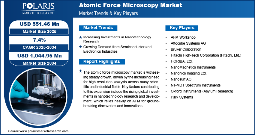
Segmental Insights
Offering Analysis
Based on offering, the segmentation includes atomic force microscopes, probes, and software. The atomic force microscopes segment held the largest share in 2025. The AFM instrument is the core component, essential for any nanoscale imaging or manipulation. Continuous advancements in AFM technology, such as improved resolution, faster scanning speeds, and enhanced functionality, contribute to its substantial presence. Manufacturers are consistently innovating to develop more versatile and user-friendly AFM systems that cater to a wider range of research and industrial applications, from material science and semiconductors to life sciences. The high initial investment required for these sophisticated instruments also contributes to this segment's significant revenue contribution.
The software segment is anticipated to register the highest growth rate during the forecast period. This rapid expansion is driven by the increasing importance of advanced data analysis, automation, and user-friendly interfaces in modern AFM applications. As AFMs become more integrated into high-throughput environments and demand more complex data interpretation, the role of specialized software becomes crucial. Microscope software innovations, including those incorporating artificial intelligence and machine learning, are enabling more efficient data processing, automated image analysis, and even predictive capabilities. These advancements enhance the performance and accessibility of AFM systems, as well as reduce the time and expertise required for operation.
Grade Analysis
Based on grade, the segmentation includes industrial and research. The industrial segment held a larger share in 2025, driven by the widespread and increasing adoption of AFMs in various industrial settings, particularly in the semiconductor, electronics, and advanced materials manufacturing sectors. Industrial-grade AFMs are designed for robust performance, high throughput, and often include automation features to meet the stringent demands of quality control, process monitoring, and research and development in these industries. The miniaturization of electronic components, the need for precise defect analysis, and the development of new materials with specific surface properties all contribute to the significant investments in industrial AFM systems.
The research segment is anticipated to register the highest growth rate during the forecast period. This accelerated growth is primarily fueled by continuous advancements in scientific research across diverse fields such as nanotechnology, life sciences, physics, and chemistry. Research-grade AFMs are often at the forefront of technological innovation, offering higher resolution, greater sensitivity, and more specialized modes of operation for complex experimental setups. The increasing global investments in academic research and the expansion of university and government laboratories drive the demand for these sophisticated instruments. Furthermore, the ability of AFMs to provide detailed insights into biological processes, material properties at the nanoscale, and the development of novel nanomaterials positions them as indispensable tools for groundbreaking discoveries.
Application Analysis
Based on application, the segmentation includes semiconductors & electronics, material science & nanotechnology, chemical & polymer research, life sciences & biomedical, and others. The semiconductors & electronics segment held the largest share in 2025, due to the critical role AFM plays in the relentless miniaturization and increasing complexity of electronic devices. As semiconductor manufacturers push for smaller feature sizes and more intricate designs, the need for precise metrology and defect inspection at the nanoscale becomes paramount. AFMs are indispensable for tasks such as characterizing surface roughness of wafers, measuring critical dimensions of circuits, and identifying subtle defects that could impact device performance. Their ability to provide non-destructive, high-resolution topographical and material property information makes them a vital tool in both research and development and quality control within this area.
The life sciences & biomedical segment is anticipated to register the highest growth rate during the forecast period. This rapid expansion is driven by the increasing application of AFM in biological research, drug discovery, and medical diagnostics. AFMs offer unique capabilities for studying biological samples, such as cells, proteins, and DNA, at their native conditions and at molecular resolution. This enables researchers to comprehend complex biological processes, investigate disease mechanisms, and develop innovative therapies. For instance, AFMs are used to analyze the mechanical properties of cells, visualize protein-protein interactions, and study the effects of drugs on biological structures.
Source: Polaris Market Research Analysis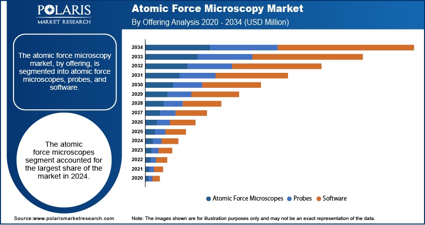
Regional Analysis
The North America atomic force microscopy market accounted for the largest share in 2025. This is mainly attributed to the region's strong focus on advanced scientific research, especially in nanotechnology and materials science. There are many universities, research institutions, and leading technology companies in North America that invest heavily in research and development, which drives the demand for advanced AFM instruments. The robust semiconductor and electronics industries in this region also contribute significantly, as they rely on AFM for crucial quality control and process development. The presence of major AFM manufacturers and a well-established infrastructure for technological innovation further support the market's growth in North America.
U.S. Atomic Force Microscopy Market Insight
The U.S. is a key player in the North America atomic force microscopy market. Its dominance is largely attributed to substantial government funding for scientific research and a vibrant ecosystem of innovation. The U.S. National Nanotechnology Initiative has continuously provided significant financial support for nanotechnology research, directly boosting the demand for advanced characterization tools such as AFMs. Moreover, the country's leading position in the semiconductor sector, coupled with ongoing advancements in biotechnology and life sciences, creates a high demand for precise nanoscale imaging and analysis. The presence of numerous academic and industrial research centers ensures a constant need for sophisticated AFM technology to drive new discoveries and industrial applications.
Europe Atomic Force Microscopy Market Trends
Europe is another major region in the atomic force microscopy market, characterized by its strong academic and research base, along with a focus on advanced manufacturing and material science. Countries across Europe have a long history of scientific excellence and continue to invest in high-tech research infrastructure. This investment supports the widespread adoption of AFMs in various scientific disciplines, including physics, chemistry, and engineering. The region's emphasis on developing novel materials and its strong automotive and aerospace industries also contribute to the demand for precise surface characterization provided by AFM technology.
In Europe, the Germany atomic force microscope market stands out as a significant contributor. The country is known for its robust research and development activities and a strong industrial sector, particularly in manufacturing, electronics, and scientific instrumentation. German universities and research institutes are at the forefront of nanotechnology and materials science research, leading to a consistent demand for advanced AFM systems. Furthermore, the presence of various key players in the microscopy and precision instrument manufacturing sectors within Germany helps drive innovation and the availability of AFM technology in the region.
Asia Pacific Atomic Force Microscopy Market Overview
Asia Pacific is rapidly emerging as a dynamic and fast-growing for atomic force microscopy. This growth is fueled by increasing investments in research and development, particularly in countries with expanding semiconductor manufacturing capabilities and strong national nanotechnology initiatives. The region's rapid industrialization, coupled with a growing focus on technological advancement and innovation, is creating a requirement for AFM instruments across a wide array of applications. The rising number of academic institutions and research laboratories, along with government support for scientific exploration, are key factors driving the expansion in Asia Pacific.
China Atomic Force Microscope Market Outlook
China is a prominent country in Asia Pacific, showcasing remarkable growth. The country's strong commitment to becoming a global leader in scientific and technological innovation has led to significant investments in advanced research infrastructure and high-tech industries. Its burgeoning semiconductor and electronics manufacturing sectors heavily rely on AFM for quality control and process optimization. Additionally, the increasing research activities in nanotechnology, materials science, and life sciences within China contribute significantly to the demand for sophisticated AFM equipment.
Source: Polaris Market Research Analysis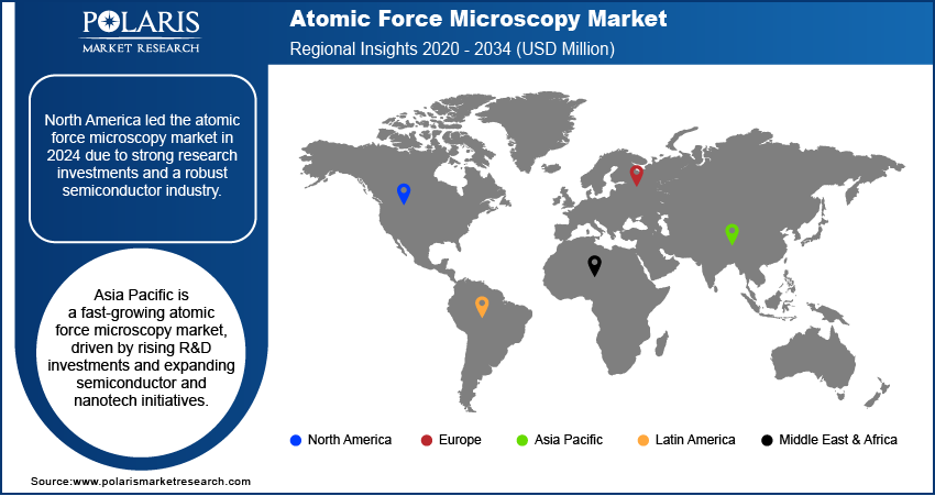
Key Players and Competitive Insights
The field of atomic force microscopy is characterized by intense competition among a few key players. These major companies, including Bruker Corporation, Park Systems, Oxford Instruments (Asylum Research), Hitachi High-Tech Corporation, Nanosurf AG, HORIBA, Ltd., and NT-MDT Spectrum Instruments, continuously innovate to offer more advanced and user-friendly AFM systems. The competitive landscape is shaped by ongoing technological developments, such as higher resolution imaging, faster scanning speeds, and integrated multi-modal capabilities. Companies are also focusing on providing specialized solutions for niche applications, alongside comprehensive support and service networks, to gain a larger share. This competitive environment drives continuous improvement in AFM technology and expands its applicability across various scientific and industrial fields.
A few prominent companies in the industry include Bruker Corporation, Park Systems, Oxford Instruments (Asylum Research), Hitachi High-Tech Corporation (Hitachi, Ltd.), Nanosurf AG, HORIBA, Ltd., NT-MDT Spectrum Instruments, AFM Workshop, Attocube Systems AG, NanoMagnetics Instruments, and Nanonics Imaging Ltd.
Key Players
- AFM Workshop
- Attocube Systems AG
- Bruker Corporation
- Hitachi High-Tech Corporation (Hitachi, Ltd.)
- HORIBA, Ltd.
- NanoMagnetics Instruments
- Nanonics Imaging Ltd.
- Nanosurf AG
- NT-MDT Spectrum Instruments
- Oxford Instruments (Asylum Research)
- Park Systems
Industry Developments
-
April 2026: Bruker Corporation announced accelerated development of its photothermal AFM-IR spectroscopy capabilities. The company stated that these advancements are aimed at addressing challenges in next-generation semiconductor technologies. They include EUV photoresist patterning and advanced materials for transistor scaling. (source: bruker.com)
-
April 2026: Park Systems inaugurated its new global headquarters in Gwacheon Knowledge & Information Town, South Korea. As per Park Systems, the building has an extensive underground cleanroom that can produce up to 35 metrology systems to meet increased demand. (source: parksystems.com)
- May 2025: A UK company released the Jupiter Discovery AFM. This new system for large samples can take high-resolution pictures, process them quickly, and repeat them well. Its simple design makes it easy for researchers to get accurate measurements. (Source: oxinst.com)
Atomic Force Microscopy Market Segmentation
By Offering Outlook (Revenue – USD Million, 2021–2034)
- Atomic Force Microscopes
- Probes
- Software
By Grade Outlook (Revenue – USD Million, 2021–2034)
- Industrial
- Research
By Application Outlook (Revenue – USD Million, 2021–2034)
- Semiconductors & Electronics
- Material Science & Nanotechnology
- Chemical & Polymer Research
- Life Sciences & Biomedical
- Others
By Regional Outlook (Revenue-USD Million, 2021–2034)
- North America
- U.S.
- Canada
- Europe
- Germany
- France
- UK
- Italy
- Spain
- Netherlands
- Russia
- Rest of Europe
- Asia Pacific
- China
- Japan
- India
- Malaysia
- Suth Korea
- Indnesia
- Australia
- Vietnam
- Rest of Asia Pacific
- Middle East & Africa
- Saudi Arabia
- UAE
- Israel
- Suth Africa
- Rest of Middle East & Africa
- Latin America
- Mexic
- Brazil
- Argentina
- Rest of Latin America
Atomic Force Microscopy Market Report Scope
| Report Attributes | Details |
| Market Size in 2025 | USD 550.63 million |
| Market Size in 2026 | USD 589.40 million |
| Revenue Forecast by 2034 | USD 1,046.87 million |
| CAGR | 7.4% from 2026 to 2034 |
| Base Year | 2025 |
| Historical Data | 2021–2024 |
| Forecast Period | 2026–2034 |
| Quantitative Units | Revenue in USD million and CAGR from 2026 to 2034 |
| Report Coverage | Revenue Forecast, Competitive Landscape, Growth Factors, and Industry Insights |
| Segments Covered |
|
| Regional Scope |
|
| Competitive Landscape |
|
| Report Format |
|
| Customization | Report customization as per your requirements with respect to countries, regions, and segmentation. |
Source: Polaris Market Research Analysis
FAQ's
The global market size was valued at USD 550.63 million in 2025 and is projected to grow to USD 1,046.87 million by 2034.
The global market is projected to register a CAGR of 7.4% during the forecast period.
North America dominated the market share in 2025.
A few key players in the market include Bruker Corporation, Park Systems, Oxford Instruments (Asylum Research), Hitachi High-Tech Corporation (Hitachi, Ltd.), Nanosurf AG, HORIBA, Ltd., NT-MDT Spectrum Instruments, AFM Workshop, Attocube Systems AG, NanoMagnetics Instruments, and Nanonics Imaging Ltd.
The atomic force microscopes segment accounted for the largest share in 2025.
The research segment is expected to witness faster growth during the forecast period.
Download Sample Report of Atomic Force Microscopy Market
Please fill out the form to request a customized copy of the research report.
