
Global Nanopatterning Market Size, Share Analysis Report, 2023-2032
REPORT DETAILS
The global nanopatterning market was valued at USD 2,005.38 million in 2022 and is expected to grow at a CAGR of 15.5% during the forecast period. A high-potential field of nanotechnology is Nanopatterning. Controlling a substance's behavior and structure at an intermediate, nanoscale level ranging between 1nm and 100 nm is essential to the science of Nanopatterning. In a larger sense, Nanopatterning is comparable to nanolithography, including several lights- or radiation-based techniques to imprint microscopic designs on materials like silicon chips. One major benefit of the nanopatterning technique is precise and accurate functioning. The technology also offers great dependability, low power consumption, cost-effectiveness, and efficiency. The process of miniaturization is facilitated by technology. Biotechnology, polymer electronics, nanoelectronics, photonics, sensors, hard drives, and microfluidic devices are just a few domains where Nanopatterning has applications.
Source: Polaris Market Research Analysis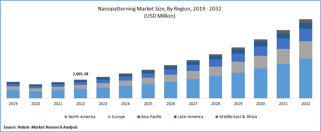
To Understand More About this Research: Download Sample Report
With the development of novel technologies like 3D Nanopatterning, the demand for electronic sensors, biomedical electronics, and nano-optics is predicted to increase, propelling the worldwide market over the forecast period. The production of photonics using Nanopatterning is expected to provide considerable cost benefits, which will help fuel industry expansion. Also, nanopatterning technology will benefit from new prospects by using Nanograft technology to treat coronary heart disease throughout the projected period.
Another factor for market growth is the expansion of the market will be fueled by the rising usage of semiconductor devices in cars. The need for semiconductor chips has surged due to the electrification and automation of vehicles. In automotive applications, several semiconductor ICs are utilized for airbag control, GPS, anti-lock brake systems, automobile navigation and display, power doors and windows, entertainment, autonomous driving, and collision detection technologies.
For instance, in June 2020, The joint venture between Micro Resist Technology GmbH and SÜSS MicroTec SE, a provider of process solutions and equipment for the semiconductor sector, was announced. Through this partnership, Micro Resist Technology will be able to adopt nanoimprint lithography, increase its manufacturing capacity, and comprehend rapidly developing needs. Throughout the forecast, the market will expand along with the rise in vehicle manufacturing. This will increase demand for semiconductor devices, which will subsequently increase demand for nanopatterning systems throughout the predicted period.
Moreover, APAC's IT and automotive sales were negatively impacted in 2020 due to lockdowns brought on by the COVID-19 epidemic and societal norms that discouraged car ownership. Also, the region's sales of Electronics and autos were hurt by supply chain disruptions brought on by the limitations on mobility. The launch of vaccination campaigns, a decline in the number of COVID-19 cases each day, the lifting of lockdown restrictions, and an increase in car manufacturing in the area all contributed to a partial recovery in vehicle sales in 2021. The market for Nanopatterning is anticipated to increase throughout the projected period.
Source: Polaris Market Research Analysis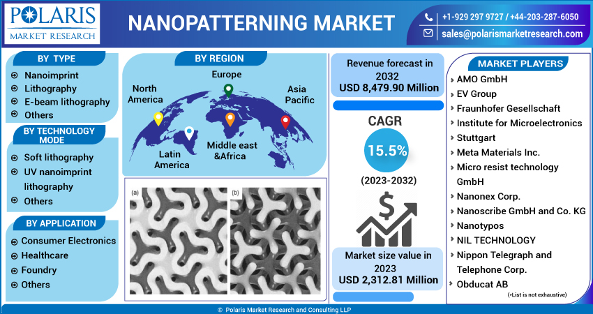
For Specific Research Requirements, Request Customization
Industry Dynamics
Growth Drivers
One of the main reasons propelling the expansion of the worldwide nanopatterning market is the introduction of high-tech consumer goods. The consumer electronics sector has seen many changes in the past five years. Smartphones have taken the place of feature phones, while laptops have taken the place of PCs. Tablets are currently quickly replacing laptops. Similar to how LED and smart Televisions are displacing CRT TVs. Manufacturers and application developers are now seeking to accelerate this transition by integrating all of these home appliances and turning them into a unified entity known as smart homes. Applications put on cell phones will be used to operate these smart houses. Manufacturers are releasing apps with rich content that can be accessed using the high-speed Internet that is now available.
As a result of these advancements and customer desire for better electronics, manufacturers are continually working to provide better consumer goods with enhanced functions. Consumer electronics devices must constantly improve in design, processing speed, power consumption, and user interface to get a larger market share during this advanced revolution. Thus, developing cutting-edge consumer electronics will fuel the expansion of the worldwide nanopatterning market during the projected period.
Report Segmentation
The market is primarily segmented based on type, technology mode, application, and region.
| By Type | By Technology Mode | By Application | By Region |
|
|
|
|
Source: Polaris Market Research Analysis
For Specific Research Requirements: Request for Customized Report
The nanoimprint segment is expected to witness the fastest growth during the forecast period
A technique for creating patterns at the nanoscale scale is called nanoimprint lithography. It is a straightforward, low-cost, high-throughput, and high-resolution nanolithography method. It produces prints by mechanically deforming the imprint resist and using subsequent techniques. During imprinting, the imprint resist is often a monomer or polymer formulation heated or exposed to UV radiation to cure.
As semiconductors must now perform better, there is worry over rising power consumption during production to increase processing speed through pattern shrinking and circuit integration. Moreover, as a technological need to support the semiconductor industry, which is anticipated to grow due to the bolstering of digital infrastructure advocated by the Japanese government, lowering power consumption during manufacture is unavoidable.
E-Beam lithography segment industry accounted for the largest market share in 2022
E-beam lithography is often referred to as direct-write lithography or maskless lithography. With resolutions lower than 10nm, the e-beam directly prints patterns on a wafer. It is appealing because it makes it possible to achieve fine solutions without a photomask. Yet, the throughputs in e-beam lithography could be better. Moreover, e-beam technology is employed for inspection, especially to quicken the yield learning procedure. This method aims to identify and remove each sort of flaw one at a time until a product can be made as specified. Although e-beam is perfect for specific fault kinds, it still has speed issues that make it unlikely to take the role of optical inspection. It works well for physical defect detection and the more conventional voltage contrast method (where the non-contact electrical defect signal may significantly shorten detection time), especially in cutting-edge technology nodes.
The demand in North America is expected to witness significant growth during projected period
North America is predicted to grow significantly during the forecast period due to the region's abundance of IC (integrated circuit) and IDM manufacturing businesses. Also, the substantial expenditures made by the telecom and electronics industry are anticipated to boost market expansion. Also, several suppliers of nanopatterning technology and the effective use of nanotechnologies in medicine support the region's supremacy.
The market for Asian nanopatterning is predicted to increase rapidly due to the rising use of advanced processors and semiconductors in various applications. The region's numerous semiconductor foundries are a major driving force behind the usage of nanopatterning. Moreover, the market in nations like China, South Korea, and India is expected to be stimulated by the technology's expanding use in fabrication processes. Due to the limited number of manufacturers, lack of access to cutting-edge technology in the area, and lithography development, this technique's usage is increasing.
Competitive Insight
Some of the major players working in the global market include AMO GmbH, EV Group, Fraunhofer Society, Meta Materials, Micro Resist Technology, NanoPattern Technologies, Nanonex Corporation, Nanoscribe, Nanotypos, NIL TECHNOLOGY, Nippon Telegraph, Obducat, Raith, ReAx Biotechnologies, SET Corp., SUSS MICROTEC, SVG Optronics, Transfer Devices, Toppan Printing, & Vistec Electron Beam.
Recent Developments
- In February 2024, Intel Corporation introduced its new Intel PentoniQ technology, leveraging advanced nanopatterning methods to produce transistors with exceptional precision and density. This advancement represents a major step toward achieving Intel’s 7nm and next-generation technology nodes.
- In May 2024, ASML Holding NV, a prominent supplier of photolithography equipment, revealed a strategic partnership with Tokyo Electron Limited to co-develop extreme ultraviolet (EUV) lithography systems for large-scale semiconductor production using nanopatterning technology. The collaboration aims to speed up EUV adoption and lower manufacturing costs across the semiconductor industry.
- In January 2021, two businesses, NanoPattern Technologies & ReAx Biotechnologies, were selected by the Polsky Center for Entrepreneurship & Innovation for investment in the George Shultz Innovation Fund, & around 150,000 was given to each team. NanoPattern Technologies will promote the sale of a photo-patternable quantum dot-ink that will help produce displays.
Nanopatterning Market Report Scope
| Report Attributes | Details |
| Market size value in 2023 | USD 2,312.81 million |
| Revenue forecast in 2032 | USD 8,479.90 million |
| CAGR | 15.5% from 2023- 2032 |
| Base year | 2022 |
| Historical data | 2019- 2022 |
| Forecast period | 2023- 2032 |
| Quantitative units | Revenue in USD billion and CAGR from 2023 to 2032 |
| Segments Covered | By Type, By Technology Mode, By Application, By Region |
| Regional scope | North America, Europe, Asia Pacific, Latin America; Middle East & Africa |
| Key Companies | AMO GmbH, EV Group, Fraunhofer Gesellschaft, Institute for Microelectronics Stuttgart, Meta Materials Inc., Micro resist technology GmbH, Nanonex Corp., Nanoscribe GmbH and Co. KG, Nanotypos, NIL TECHNOLOGY, Nippon Telegraph and Telephone Corp., Obducat AB, Raith GmbH, SET Corp. SA, SUSS MICROTEC SE, SVG Optronics Co. Ltd., Toppan Printing Co. Ltd, Transfer Devices Inc., Upper Austrian Research GmbH, and Vistec Electron Beam GmbH |
Source: Polaris Market Research Analysis
Nanopatterning Market FAQ's
key companies in nanopatterning market are AMO GmbH, EV Group, Fraunhofer Society, Meta Materials, Micro Resist Technology, NanoPattern Technologies.
The global nanopatterning market expected to grow at a CAGR of 15.5% during the forecast period.
The nanopatterning market report covering key segments are type, technology mode, application, and region.
key driving factors in nanopatterning market are rising demand for surface customization at nanoscale.
The global nanopatterning market size is expected to reach USD 8,479.90 million by 2032.
Download Sample Report of Nanopatterning Market
Please fill out the form to request a customized copy of the research report.
