
Pellicle Market Size, Share, Trends & Forecast, 2026–2034
REPORT DETAILS
Pellicle Market Summary
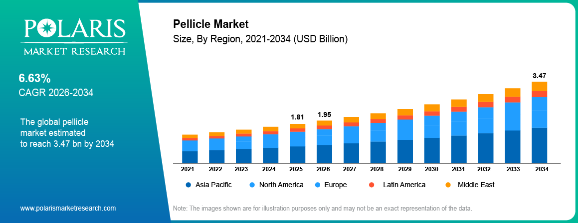
Pellicle market size was valued at USD 1.81 billion in 2025. The market is expected to register a CAGR of 6.63% from 2026 to 2034. Growth is driven by rising semiconductor production and increasing EUV adoption. Also, advanced chip manufacturing and next-generation pellicle technologies fuel the market expansion.
Market Statistics
Pellicle Market Key Takeaways
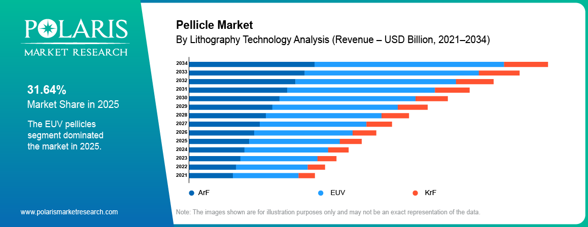
- Asia Pacific dominated the market with 39.72 % share in 2025 on account of robust semiconductor manufacturing in the region.
- The North America pellicle market is projected to register a CAGR of 6.21% during the forecast period. The market growth is driven by increasing investments in advanced semiconductor manufacturing and domestic chip capacity.
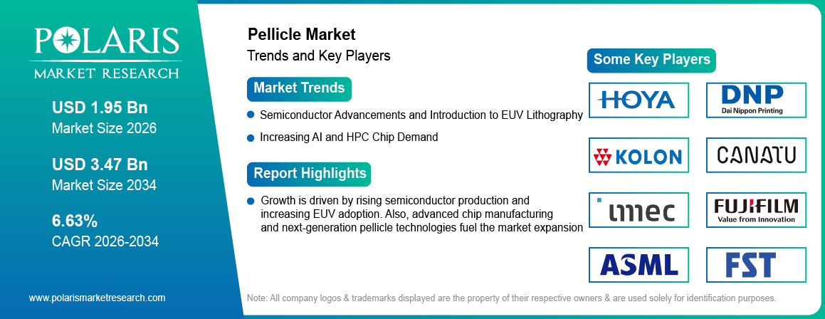
- EUV pellicles held 31.64 % market share in 2025 due to rising adoption of EUV lithography technology in semiconductor manufacturing.
- The ArF pellicles market is expected to register an 5.48% CAGR during the forecast period.
- The >95% segment held the largest share of 48.62% in 2025. Rising use of EUV and High-NA EUV lithography fuels the development of thin, robust membranes with high optical transmission.
Note: Figures and projections outlined in this report are the result of Polaris Market Research’s proprietary analytical processes, grounded in the latest available datasets and market observations.
What are Pellicles?
The pellicle market comprises thin protective membranes used over semiconductor photomasks or reticles to reduce the risk of particle contamination during lithography. The semiconductor pellicle is used to separate the reticle surface from the airborne contaminants and thus prevents the particles from being printed on the wafer during exposure. Therefore, pellicles are an essential part of reticle protection, particularly as semiconductor manufacturers move toward smaller process nodes and more demanding lithography needs.
Demand is closely linked to semiconductor manufacturing activity, particularly advanced logic, foundry, DRAM, high-bandwidth memory, and other applications requiring leading-edge lithography. The Semiconductor Industry Association reports global semiconductor sales of USD 791.7 billion in 2025, up 25.6% from 2024. The association also reported that global sales were continuing to accelerate during 2026 (Source: semiconductors.org).
Semiconductor manufacturing investment is also supporting the long-term opportunity. SEMI projects global 300mm front-end fab equipment spending to reach a record USD 149 billion in 2026, while installed 300mm capacity is expected to continue increasing through 2029. Such capacity additions expand the addressable base for photomasks and pellicles used in advanced lithography processes (Source: semi.org).
The transition toward EUV and High-NA EUV is creating additional technical requirements. ASML's High-NA EUV platform increases numerical aperture from 0.33 to 0.55 and is designed to support future advanced logic and memory nodes. The company reported that the first full-specification TWINSCAN EXE:5200B was delivered in 2025, while its 2025 annual report indicates that the EXE platform is expected to support high-volume manufacturing from 2027.
How a Semiconductor Pellicle Works
A semiconductor pellicle protects a photomask during lithography through a relatively simple physical principle.
1. Pellicle Mounting
The membrane is stretched on a frame and is positioned above the photomask or reticle. The frame maintains a controlled spacing between the pellicle and the patterned mask surface.
2. Particle Interception
Particles in the lithography environment may deposit on the pellicle membrane rather than directly to the photomask. This makes it unlikely that the particle is a defect in the printed image.
3. Light Transmission
The light for exposure goes through the pellicle before it reaches the photomask. The membrane should be optically sufficiently transmissive not to interfere with the lithography process.
4. Pattern Transfer
The lithography system transfers the photomask pattern onto the wafer. The particle remains separated from the patterned surface, reducing its effect on the projected image.
5. Thermal Management
The pellicle absorbs part of the exposure energy. EUV pellicles therefore need to manage heat while retaining their mechanical and optical properties.
6. Inspection and Maintenance
Pellicles can be checked for defect, contamination, damage and change in optical performance. The more demanding the exposure conditions are, the more important inspection becomes.
Extreme ultraviolet (EUV) lithography works at 13.5 nm and requires pellicles with high EUV transmittance, low defectivity, adequate mechanical strength, and resistance to thermal loading, making the EUV pellicle market more prominent. More exposure power and higher lithography resolution lead to more pronounced performance limitations of conventional pellicle materials. This is encouraging development of silicon-based membranes, silicon nitride membranes, polysilicon membrane, and carbon nanotube (CNT) pellicles.
EUV Pellicles vs DUV Pellicles
| Attribute | EUV Pellicle | DUV Pellicle |
| Exposure wavelength | 13.5 nm | 193 nm (ArF) / 248 nm (KrF) |
| Membrane thickness | 30–50 nm | 800–1,000 nm |
| Common materials | Polysilicon, silicon nitride, carbon nanotube (CNT) | Fluoropolymer |
| Transmittance target | ~90%+ (up to 92% at 13.5 nm) | High, but less thermally constrained |
| Thermal load | High — thermal stability above 1,000 W/m² absorbed power | Comparatively low |
| Manufacturing complexity | High — sub-50nm defect-free film fabrication | Lower — mature, established process |
| Typical application | Advanced logic/memory nodes below 7nm | Legacy nodes, automotive/industrial ICs |
Source: Polaris Market Research Analysis
Market Dynamics
Driver: Semiconductor Advancements and Introduction to EUV Lithography
The semiconductor industry is undergoing a profound transformation, driven by advancements in technologies such as artificial intelligence, the Internet of Things, 5G, and electrified vehicles. These innovations have led to a surge in demand for high-quality, high-yield chips across various industry verticals. In response to this growing need, leading semiconductor manufacturers are investing in the development and production of cutting-edge semiconductors. For instance, that 5G subscriptions will reach 6.4 billion globally by 2031, representing two-thirds of all mobile subscriptions (Source: ericsson.com).
One pivotal advancement in this context is the introduction of Extreme Ultraviolet (EUV) lithography. EUV lithography enables the production of smaller, more efficient, and higher-performance semiconductor chips. This technology enhances the precision and capabilities of semiconductor manufacturing, driving the demand for pellicles.
Pellicles are essential components in the semiconductor manufacturing process, as they protect semiconductor wafers from contamination during photolithography. The integration of EUV lithography has further intensified the need for high-quality pellicles to ensure the flawless production of advanced semiconductor chips. Consequently, the Pellicle Market is experiencing significant growth, bolstered by the semiconductor industry's relentless pursuit of innovation and excellence.
Driver: Increasing AI and HPC Chip Demand
The surge in demand for artificial intelligence (AI) and HPC chips is indirectly boosting the semiconductor pellicle market, as the more advanced processors require more complex semiconductor fabrication processes. AI accelerators, GPUs, CPUs and high performance memory are increasingly produced using advanced logic and EUV lithography, making photomask pellicles even more critical to contamination control and semiconductor yield. As we advance to High-NA EUV and advanced logic nodes, the requirements for EUV pellicle performance, such as high EUV transmittance, thermal stability, mechanical strength and particle defect control, continue to increase.
The rise of chiplet-based architectures is also helping the broader advanced-chip ecosystem. Arteris introduced FlexGen Multi-Die in Sept 2026 to address data movement for AI and HPC applications for chiplet-based architectures. These trends are driving demand for advanced logic and memory manufacturing that indirectly benefits EUV lithography pellicles, High-NA EUV pellicles and advanced reticle protection technologies. The relationship is particularly important because higher performance chips require more complex lithography and tighter photomask contamination control. This means that continued investment in AI and HPC semiconductors is expected to create opportunities for high-performance pellicles with greater transmission, durability and thermal performance (Source: globenewswire.com).
Restraint: High Manufacturing Complexity and Thermal Requirements
The manufacturing of the pellicle requires very tight control of the membrane thickness, optical transmission, mechanical strength, surface quality and defect levels. For EUV lithography, these requirements are even more demanding as the membrane has to transmit sufficient 13.5 nm radiation while being structurally sound under high exposure conditions. Therefore, EUV pellicles require careful optimization of membrane materials, thickness, permeability, thermal properties and contamination control. High power EUV scanners may result in higher heat absorption by the membrane, which poses challenges in thermal deformation, material degradation and transmission stability. These requirements increase the manufacturing complexity and can add to the production cost as compared to conventional DUV pellicles.
Likewise, new carbon nanotube (CNT) pellicles need thorough testing and qualification prior to wider commercial deployment. Canatu’s CNT100 SEMI reactor was approved by customers in July 2025. However, the full coated CNT pellicle needs further customer approvals before pilot and risk production can move into high-volume manufacturing. FINE SEMITECH received a commercial production license from Canatu in October 2025 and announced a further CNT100 SEMI reactor order in August 2026. Such qualification requirements can extend commercialization timelines and create barriers for new suppliers, thus limiting the pellicle market growth rate.
Opportunity: High-NA EUV Transition and CNT Pellicle Commercialization
The transition to high-NA EUV lithography is fueling the progress of next-generation semiconductor pellicles with higher transmission, improved thermal performance and increased mechanical strength. In March 2026, imec acquired ASML EXE:5200 High-NA EUV system being used to advance sub-2nm logic and high-density memory technologies. As semiconductor manufacturers move to more advanced logic and memory nodes, the demands on High-NA EUV pellicles are increasing, particularly in the areas of EUV transmittance, thermal stability, particle control, and membrane lifetime (Source: imec-int.com).
Another significant opportunity is the commercialization of CNT pellicles. In 2025, Canatu’s CNT100 SEMI reactor was approved for mass production of CNT pellicle membranes by a customer and was then awarded a commercial production license for FINE SEMITECH. In August 2026, Canatu announced a further reactor order from FINE SEMITECH to increase capacity for manufacturing of CNT pellicles. CNT membranes can offer high EUV transmission and thermal resistance, which is relevant to high power EUV applications. These developments are expected to create opportunities for CNT pellicles for EUV lithography, advanced reticle protection, and next-generation photomask contamination control.
Challenges in Pellicle Manufacturing
The manufacture of pellicles requires highly controlled processes covering membrane formation, thickness control, frame assembly, cleaning, inspection, and packaging. The challenge increases for EUV pellicles because membranes must combine high EUV transmittance with mechanical strength, thermal stability, and low defectivity under high-energy exposure conditions. High-power EUV and emerging High-NA EUV systems place additional requirements on membrane durability and dimensional stability. The maintenance of uniform membrane thickness and surface quality is important because microscopic defects can affect transmission, create contamination risks and lower the yield of semiconductors. So manufacturers must be stringent in photomask contamination and particle defect control throughout production. Also, the inconsistent cost and availability of semiconductor & IC packaging materials may lead to market challenges.
CNT pellicles pose other scale-up challenges, as manufacturers have to develop repeatable methods for deposition, processing, inspection and assembly, while controlling production costs. Commercialization also needs customer qualification and compatibility with advanced lithography systems. These can increase the manufacturing complexity and prolong the qualification timelines, especially for next generation carbon nanotube pellicles for EUV lithography. Suppliers must also balance transmission, thermal performance, mechanical strength, defectivity and production yield to achieve commercially viable pellicles for advanced semiconductor manufacturing.
Key Areas of Pellicle Market
Pellicles for High-NA EUV Lithography
High-NA EUV lithography is increasing the technical requirements placed on photomask and pellicle systems. ASML's TWINSCAN EXE:5000 uses a 0.55 NA optical system and is designed to print smaller features with fewer patterning steps. ASML states that the platform can support future 2 nm logic applications and subsequent memory nodes.
High-NA EUV pellicles must balance optical transmission with mechanical and thermal performance. Increasing EUV source power can raise the thermal load experienced by the membrane. Pellicle failure modes such as transmission loss, deformation, particle generation and accelerated material degradation can reduce lithography productivity and yield.
The change also is linked to shifts in mask infrastructure. ASML and TSMC announced an industry initiative in September 2026 to move to 12-inch photomasks for High-NA EUV, with a pilot line targeted for 2031 and broader system readiness targeted for 2033. Samsung separately announced participation in a 12-inch photomask initiative and planned High-NA EUV adoption for future DRAM manufacturing.
These developments indicate that the pellicle ecosystem will need to evolve alongside mask formats, lithography systems, inspection technologies, and advanced-node manufacturing processes.
Carbon Nanotube Pellicles for EUV Lithography
Carbon nanotube pellicles are emerging as an important technology for next-generation EUV lithography because CNT membranes can combine high EUV transmission, mechanical strength, thermal stability, and low optical scattering.
Research and industry development have increasingly shifted toward full-size CNT membranes and production-scale manufacturing. In July 2025, Canatu announced customer approval for its CNT100 SEMI reactor and post-processing equipment, describing the qualification as enabling mass production of CNT pellicle membranes. The company later reported that a commercial production license had been granted to FST and that further reactor orders were supporting expansion of CNT pellicle manufacturing capacity (Source: mitsuichemicals.com).
LINTEC reported in February 2026 that it had developed a coating formulation to improve CNT pellicle durability and had established mass-production technology for a dual-density CNT pellicle design. The company is also working with AIST on technologies for establishing an initial mass-production system.
The main technical challenges remain durability, hydrogen-radical resistance, particle control, coating stability, transmission uniformity, mechanical robustness, and lifetime. Continued improvement in these areas will determine the pace at which CNT pellicles move from qualification to broader high-volume manufacturing.
Silicon-Based vs. CNT EUV Pellicles
| Attribute | Silicon-Based (Polysilicon/SiN) | Carbon Nanotube (CNT) |
| Transmittance | Up to ~90% | Targeting 91%+ |
| Thermal resilience | Adequate for current-power EUV | Designed for high-power/High-NA EUV systems |
| Commercialization maturity | In active production (Shin-Etsu, Mitsui Chemicals, Inc., SKC) | Emerging — Canatu CNT100 reactor received customer approval and a commercial production license in 2025; Mitsui targeting ~5,000 sheets/year capacity, completion around end-2025 |
| Primary developers | Shin-Etsu Chemical, Mitsui Chemicals, Inc., SKC | Canatu, Mitsui Chemicals, Inc. (imec collaboration) |
| Best fit | Current-generation 0.33 NA EUV lines | Next-generation high-power and 0.55 NA High-NA EUV lines |
Source: Polaris Market Research Analysis
High-Power EUV and Pellicle Requirements
Increasing EUV source power places greater thermal and mechanical demands on the pellicle. The membrane absorbs a portion of incident EUV energy, which can raise its operating temperature and accelerate material degradation. Excessive thermal loading can affect membrane stability, EUV transmittance, flatness, and operating lifetime. These challenges become more important as semiconductor manufacturers adopt advanced EUV and High-NA EUV lithography for smaller logic and memory nodes. Therefore, high-power EUV pellicles need to combine high EUV transmittance with low absorption, strong mechanical properties, efficient thermal radiation, and resistance to the scanner environment.
Exposure to hydrogen radicals is also a major concern as the reactive species can affect the susceptible membrane materials during the EUV operation. This is driving the development of new materials and coatings such as CNT pellicles with enhanced durability in harsh exposure environments. LINTEC has developed a double density CNT pellicle structure to increase the membrane thickness in peripheral areas to improve durability. These developments are aiding the evolution of pellicles for high power EUV and High-NA EUV pellicle requirements.
Role of Pellicles in Photomask Protection
In lithography for semiconductors, pellicles are used to protect the reticle by creating a controlled physical barrier on top of the photomask. A thin membrane is placed over the patterned mask that permits exposure light to pass through but blocks airborne particles and other contaminants from reaching the surface of the mask directly. The particles deposited on the pellicle are out of the main focal plane, and therefore reduce their possible impact on the pattern transferred to the wafer. This positions the photomask pellicle as an important component of contamination control strategies.
As semiconductor manufacturers transition to more sophisticated nodes, particle control becomes increasingly critical as even small defects can impact wafer yield. When a photomask is contaminated, it can print the same defect on multiple wafer exposures which increases material waste and manufacturing cost. Pellicle performance therefore affects mask cleanliness, semiconductor yield, defect control, lithography productivity, and reticle lifetime. As a result, pellicles are increasingly evaluated as an integral part of the broader photomask and lithography ecosystem.
Pellicle vs. Photomask
| Feature | Pellicle | Photomask |
| Main function | Protects the photomask from particles | Contains the circuit pattern |
| Position | Mounted above the mask | Positioned inside the lithography system |
| Main material focus | Thin optical membrane | Patterned substrate and absorber structure |
| Exposure function | Transmits exposure light | Defines the pattern transferred to the wafer |
| Defect impact | Reduces particle-related mask contamination | Defects can affect printed wafer patterns |
| Replacement need | Depends on damage and process requirements | Managed through mask inspection and maintenance |
Source: Polaris Market Research Analysis
EUV Pellicle Inspection and Quality Control
EUV pellicle inspection is critical because membrane defects can affect lithography performance even when the underlying photomask is defect-free. Inspection processes have to detect particles, membrane defects, dimensional deviations, coating irregularities, tears and other abnormalities without damaging the fragile membrane. This becomes particularly important for EUV pellicles where minor variations in transmission or membrane integrity can affect exposure performance and semiconductor yield.
Quality control extends across membrane formation, coating, frame assembly, cleaning, handling, packaging, and final qualification. Key parameters include EUV transmittance, transmission uniformity, surface cleanliness, particle levels, membrane flatness, mechanical deformation, thermal behavior, and structural integrity. High-NA EUV is further increasing inspection requirements because advanced pellicles must operate under higher-performance exposure conditions. Suppliers therefore need inspection systems capable of detecting increasingly small defects while maintaining throughput. Improvements in inspection and quality control can support higher pellicle yields, reduce manufacturing losses, and improve reliability across advanced semiconductor production.
Pellicle Demand in Advanced Logic and Memory Chips
Advanced logic and memory manufacturing represents a significant demand area for high-performance pellicles because these devices increasingly depend on advanced lithography technologies. The move towards GAA transistor architectures at advanced logic nodes will require further accuracy in lithography and contamination-free photomasks. AI accelerators, GPUs, CPUs, networking processors, and other advanced logic devices require high-density semiconductor manufacturing, while DRAM and other memory technologies are being developed to support AI servers, high-performance computing, mobile devices, and data-center infrastructure. Increasing wafer production at advanced nodes consequently supports demand for EUV pellicles and advanced photomask protection.
The transition toward High-NA EUV is particularly relevant to this segment. ASML’s 0.55 NA lithography EXE platform is aimed at future advanced logic and memory applications, while Samsung announced in September 2026 plans to use High-NA EUV for future DRAM manufacturing. Such developments may increase the demand of High-NA EUV pellicles with high transmittance, thermal stability, mechanical strength and contamination resistance. The expansion of AI and HPC semiconductor production is therefore expected to indirectly support the semiconductor pellicle market through higher utilization of advanced lithography processes.
Pellicle Market Segmentation Analysis
By Lithography Technology Analysis
The EUV segment is expected to grow fastest at 9.84% during forecast period. The increasing use of EUV lithography in advanced logic and memory manufacturing requires effective photomask contamination control, which is important for maintaining semiconductor yield and process reliability. More chipmakers are also adopting EUV pellicles as they increase output in advanced nodes and broaden the use of EUV for critical lithography layers. The transition to High-NA EUV is generating additional requirements for high transmission, thermally stable and mechanically robust EUV pellicles. EUV lithography is also being used increasingly in investments in high-end semiconductor fabs, AI processors, HPC and memory tech, creating opportunities for advanced photomask pellicle technologies.
The ArF segment dominated the market with 48.72% in 2025. The continued use of ArF lithography across the spectrum of mature and advanced semiconductor manufacturing processes sustains DUV pellicle demand. ArF lithography is still important for multiple semiconductor layers and applications that do not require EUV exposure, which creates sustained demand for ArF pellicles and related reticle protection solutions. Growth in the automotive, industrial, consumer electronics and other semiconductor applications is also supporting the segment. The demand for automotive electronics, connectivity devices, sensors, power management components, and other chips continues to drive semiconductor manufacturers to expand and upgrade production capacity. The continued use of ArF lithography is expected to support demand for DUV pellicles during the forecast period.
By Performance Analysis
The ≥95% segment accounted for the largest market share of 48.62% in 2025. High transmittance pellicles protect the photomasks and reduce the optical loss during lithography exposure. The semiconductor makers are embracing advanced lithography processes, which spur demand for higher EUV transmittance and enhanced exposure efficiency. The segment is of significant importance in advanced logic and memory manufacturing, where transmission performance can affect process efficiency and semiconductor yield. The increasing use of EUV and High-NA EUV lithography is also driving the development of thin, robust membranes with high optical transmission.
Pellicle Market Regional Insights
North America Pellicle Market
North America held significant market share of 22.64% in 2025. The regional market is supported by investments in semiconductor manufacturing, government initiatives, advanced-node capacity expansion, and research activities focused on next-generation lithography. In July 2026, TSMC announced an additional USD 100 billion investment in Arizona, bringing its total planned investment in the United States to USD 265 billion and expanding its planned footprint to 12 semiconductor manufacturing and packaging facilities. The expansion includes additional advanced fabs targeting 2-nm and more advanced technologies. This expansion is expected to strengthen demand for EUV pellicles, photomask pellicles, and related contamination-control technologies as domestic production of advanced logic chips increases (Source: commerce.gov).
Europe Pellicle Market
Europe represented an 26.38% share of the global pellicle market in 2025 and is expected to grow at an 5.86% CAGR during 2026–2034. The region hosts leading lithography and semiconductor research organizations such as ASML and imec, which are developing advanced lithography technologies and materials. The European Chips Act is also driving additional demand for semiconductor manufacturing equipment and components as semiconductor capacity expands. ESMC, a joint venture of TSMC, Bosch, Infineon and NXP, is building a 300mm semiconductor fab in Dresden using FinFET technology for 28/22nm and 16/12nm processes. The plant is expected to reach 480,000 wafers a year by 2029 (Source: ec.europa.eu).
Asia Pacific Pellicle Market
The Asia Pacific region accounted for the highest market share in 2025, with 39.72%, and is expected to grow at a CAGR of 7.42% from 2026 to 2034. The region’s top position is in line with the concentration of semiconductor fabs, memory makers, foundries, photomask suppliers and semiconductor-material companies in Japan, South Korea, Taiwan, China and Singapore. Additional investment in advanced manufacturing is expanding the addressable market for EUV pellicles, DUV pellicles and other photomask protection technologies. In January 2026, Micron announced the groundbreaking of an advanced wafer fabrication facility in Singapore with an investment of around USD 24 billion over a period of 10 years with wafer production expected to start in the second half of 2028 (Source: micron.com).
Latin America Pellicle Market
Latin America had 6.12% share in the global market in 2025. The regional semiconductor ecosystem is still relatively small compared with Asia Pacific, North America and Europe, limiting the demand for advanced EUV pellicles and specialized photomask protection technologies in the short term. Demand today is being driven primarily by electronics manufacturing, industrial applications, semiconductor-related supply chain activities and supporting technology infrastructure. The region’s position in the global semiconductor value chain is gradually developing, as governments and companies look to strengthen their local electronics and technology skills.
Middle East & Africa Pellicle Market
The Middle East & Africa market is expected to register a CAGR of 7.04% during the forecast period. Investments in electronics manufacturing, industrial automation, semiconductor-related infrastructure, and technology services could create opportunities for the regional market in the coming years. Growth in semiconductor assembly, testing, and supporting component industries can indirectly increase demand for semiconductor materials and manufacturing inputs. However, adoption of advanced EUV lithography pellicles is expected to remain limited until the region develops greater leading-edge wafer fabrication capacity. Opportunities are more likely to emerge initially in supporting semiconductor supply-chain activities, DUV applications, inspection, and contamination-control solutions.
Pellicle Supply Chain and Production Capacity
The pellicle supply chain consists of membrane material developers, pellicle makers, photomask companies, lithography equipment makers, inspection companies, chipmakers and research houses. Key participants include Mitsui Chemicals, Inc., Shin-Etsu Chemical, S&S Tech, SKC and Canatu, with organizations such as imec contributing to cutting-edge lithography research and technology validation. As semiconductor makers ramp up EUV and advanced node production, the supply chain becomes more and more important and the demand for qualified photomask pellicles grows.
Production capacity is becoming a key factor for the EUV pellicle market mainly in advanced logic and memory manufacturing. Qualified pellicles shall be tested for transmission, mechanical stability, cleanliness, defectivity and compatibility with photomasks and lithography tools. Mitsui Chemicals, Inc. aims to produce some 5,000 CNT pellicle sheets annually, while Canatu has made progress in developing its CNT manufacturing technology for commercial-scale production. Expansion of specialized capacity can support the commercialization of CNT pellicles and address emerging High-NA EUV pellicle requirements.
Competitive Landscape
The global pellicle market includes pellicle manufacturers, semiconductor materials companies, photomask suppliers, lithography equipment manufacturers, inspection companies, and research organizations. Competition is increasingly based on EUV transmittance, thermal stability, membrane strength, defect control, cleanliness, production consistency, pellicle lifetime, and customer qualification capabilities. Suppliers are developing photomask pellicles that are more sophisticated to meet the stringent needs of advanced logic and memory manufacturing. The shift to EUV and High-NA EUV lithography is creating an ever-increasing need for high-performance reticle protection technologies that can enable semiconductor yield and process reliability.
The move toward next-generation lithography is also driving investment in advanced membrane materials and manufacturing processes. Carbon nanotube (CNT) pellicles are opening new avenues thanks to their potential to marry high EUV transmission, thermal robustness and mechanical strength in ultra thin membranes. Suppliers are also working on scaling up production, inspection and defect control for commercial use. Increasing demand for High-NA EUV pellicle requirements, advanced-node semiconductor manufacturing, and CNT pellicle EUV lithography is expected to intensify competition across the market through 2034.
List of Key Pellicle Companies
-
Dai Nippon Printing Co., Ltd.
-
FUJIFILM Holdings Corporation
-
FINE SEMITECH CORPORATION (FST)
-
Hoya Corporation
-
imec
-
Kolon Industries, Inc.
-
LINTEC Corporation
-
Micro Lithography, Inc.
-
Mitsubishi Materials Corporation
-
Mitsui Chemicals, Inc.
-
Photronics, Inc.
-
S&S Tech Co., Ltd.
-
Shin-Etsu Chemical Co., Ltd.
-
SKC Co., Ltd.
-
Teledyne DALSA Inc.
-
Tekscend Photomask
Market Positioning
| # | Company | HQ | Role in Pellicle Value Chain | EUV / High-NA Focus | Positioning Notes |
| 1 | Mitsui Chemicals, Inc. | Tokyo, Japan | Pellicle manufacturer (EUV + CNT) | EUV, CNT | Developed CNT pellicle technology; targeting approx. 5,000 sheets/year capacity; best-placed incumbent for scaled EUV pellicle supply. |
| 2 | Canatu | Vantaa, Finland | CNT pellicle developer | CNT, High-NA | CNT100 SEMI reactor received customer approval and a commercial production license in 2025; CNT membranes suit higher-power and High-NA roadmaps. |
| 3 | S&S Tech Co., Ltd. | South Korea | Pellicle manufacturer | EUV | Reported approx. 90.2% EUV transmittance in proprietary designs; strong Korean foundry/IDM proximity. |
| 4 | Shin-Etsu Chemical Co., Ltd. | Tokyo, Japan | Pellicle manufacturer / materials | EUV | Developing advanced silicon-based membrane technologies; deep materials and quartz/mask-blank heritage. |
| 5 | SKC Co., Ltd. | Seoul, South Korea | Pellicle manufacturer | EUV | Developing advanced EUV pellicle solutions; leverages Korean semiconductor-materials ecosystem. |
| 6 | FINE SEMITECH CORPORATION (FST) | South Korea | Pellicle manufacturer | EUV (in development) | Established mask-protection and pellicle supplier in Korea; extending into EUV pellicle development. |
| 7 | LINTEC Corporation | Tokyo, Japan | CNT sheet / pellicle material developer | CNT, EUV | Carbon-nanotube sheet capability positions it as a potential CNT pellicle membrane supplier. |
| 8 | ASML Holding N.V. | Veldhoven, Netherlands | EUV lithography equipment; pellicle technology originator | EUV, High-NA | Defines lithography ecosystem requirements and works with pellicle partners; its specifications shape pellicle qualification. |
| 9 | imec | Leuven, Belgium | Semiconductor R&D organization | CNT, High-NA | High-NA EUV validation and advanced process research; key neutral test-bed for next-generation pellicle materials. |
| 10 | Dai Nippon Printing Co., Ltd. | Tokyo, Japan | Photomask manufacturer | DUV, EUV | Major photomask supplier and a key downstream adopter and qualifier of EUV pellicles. |
| 11 | Photronics, Inc. | Brookfield, Connecticut, US | Photomask manufacturer | DUV, EUV | Largest independent photomask maker; demand-side influence on pellicle adoption. |
| 12 | Tekscend Photomask | Tokyo, Japan | Photomask manufacturer | DUV, EUV | Photomask supplier (formerly Toppan Photomasks); offers photomask-related solutions. |
| 13 | Hoya Corporation | Tokyo, Japan | Mask blanks / photomask materials | EUV | Leading EUV mask blank supplier; upstream partner in the mask-pellicle assembly chain. |
| 14 | Micro Lithography, Inc. | California, US | Pellicle / photomask supplier | DUV, EUV | Provides photomask and pellicle-related products; focused on mature-node and specialty demand. |
| 15 | FUJIFILM Holdings Corporation | Tokyo, Japan | Lithography materials supplier | EUV materials | Broad semiconductor-materials portfolio; pellicle role is adjacent rather than core. |
| 16 | Kolon Industries, Inc. | Gwacheon, South Korea | Advanced materials / films | Emerging | Advanced film and materials capabilities; potential membrane or frame-material entrant. |
| 17 | Mitsubishi Materials Corporation | Tokyo, Japan | Materials supplier | Emerging | Materials-based participation; positioning depends on component and frame-material supply. |
| 18 | Teledyne DALSA Inc. | Waterloo, Canada | Specialty MEMS / imaging manufacturer | Emerging | Specialty microfabrication capability; limited visible pellicle-specific activity. |
Source: Polaris Market Research Analysis
Recent Developments
- In May 2026, Lintec is advancing CNT-based EUV pellicle development and plans to begin mass production in 2026, backed by a reported USD 45 million investment. (Source: trendforce.com)
- In February 2026, LINTEC developed a durable dual-density CNT pellicle with an advanced coating formulation for EUV lithography and is working with AIST toward mass production. (Source: lintec-global.com)
- In August 2025, Canatu Plc invested in Lasertec’s PELMIS EUV pellicle inspection system. It is expected to enhance its metrology capabilities in the semiconductor industry. (Source: canatu.com)
- In October 2025, Samsung and S&S Tech have jointly applied for a patent for a magnetic EUV pellicle frame that will improve pellicle attachment and alignment, and reduce adhesive-related outgassing. (Source: thelec.net)
Pellicle Market Segmentation
By Lithography Technology Outlook (Revenue, USD Billion, 2021–2034)
- ArF
- EUV
- KrF
By Pellicle Type Outlook (Revenue, USD Billion, 2021–2034)
- Polymer Pellicles
- Silicon Pellicles
- Metal Pellicles
- Glass Pellicles
- Others
By Performance Outlook (Revenue, USD Billion, 2021–2034)
- ≥95%
- 90%–<95%
- 85%–<90%
- <85%
By End-Use Industry Outlook (Revenue, USD Billion, 2021–2034)
- Electronics
- Semiconductors
- Automotive
- Aerospace
- Medical Devices
By Regional Outlook (Revenue, USD Billion, 2021–2034)
- North America
- U.S.
- Canada
- Europe
- Germany
- France
- UK
- Italy
- Spain
- Netherlands
- Russia
- Rest of Europe
- Asia Pacific
- China
- Japan
- India
- Malaysia
- South Korea
- Indonesia
- Australia
- Vietnam
- Rest of Asia Pacific
- Middle East & Africa
- Saudi Arabia
- UAE
- Israel
- South Africa
- Rest of Middle East & Africa
- Latin America
- Mexico
- Brazil
- Argentina
- Rest of Latin America
Pellicle Market Report Scope
| Report Attributes | Details |
| Market Size in 2025 | USD 1.81 Billion |
| Market Size in 2026 | USD 1.95 Billion |
| Revenue Forecast by 2034 | USD 3.47 Billion |
| CAGR | 6.63% from 2026 to 2034 |
| Base Year | 2025 |
| Historical Data | 2021–2024 |
| Forecast Period | 2026–2034 |
| Quantitative Units | Revenue in USD Billion and CAGR from 2026 to 2034 |
| Report Coverage | Revenue Forecast, Competitive Landscape, Growth Factors, and Industry Trends |
| Segments Covered |
|
| Regional Scope |
|
| Competitive Landscape |
|
| Report Format |
|
| Customization | Report customization as per your requirements with respect to countries, regions, and segmentation. |
Source: Polaris Market Research Analysis
Future Outlook
The pellicle market is expected to expand through 2034 as semiconductor manufacturers increase investment in EUV, High-NA EUV, advanced logic, and memory production. Demand is expected to favor pellicles offering higher EUV transmittance, improved thermal stability, mechanical durability, and lower defect levels. Commercial production and qualification of CNT pellicles could strengthen their role in high-power EUV and next-generation lithography. The transition toward 0.55 NA systems is also creating new High-NA EUV pellicle requirements, including greater resistance to thermal stress and tighter dimensional control.
Pellicle inspection and quality control are expected to become more sophisticated as membrane structures become thinner and process tolerances tighten. Increasing demand for AI processors, high-performance computing (HPC), HBM, and advanced-node semiconductors is expected to support demand for high-performance photomask pellicles. Collaboration among pellicle manufacturers, equipment suppliers, photomask companies, research organizations, and semiconductor manufacturers will remain important for improving CNT pellicle EUV lithography, production scalability, and semiconductor yield.
Research Methodology
The pellicle market size and estimates for segments and sub-segments are developed using a combination of bottom-up and top-down approaches. The methodology considers semiconductor manufacturing activity, lithography technology adoption, pellicle demand, production capacity, pricing, regional expansion and technology developments to arrive at market estimates for 2025 and forecasts through 2034.
Secondary Research & Data Collection
Secondary research includes company annual reports, investor presentations, product announcements, patents, technical publications, industry reports, trade associations, semiconductor manufacturing data, sources on lithography technology, and information on the photomask industry. Sources are consulted to gage the progress in EUV pellicles, DUV pellicles, CNT membranes, High-NA EUV, capacity of semiconductors and activity in regional manufacturing.
Market Estimation & Modelling
The bottom-up approach looks at semiconductor production volumes, lithography adoption, pellicle utilization, replacement needs, average selling prices, manufacturing capacity and developments at the supplier level. The top-down approach considers semiconductor investment, EUV and High-NA EUV deployment, advanced logic and memory capacity, regional fab expansion and broader semiconductor market dynamics. These inputs are used to estimate the size of the semiconductor pellicle market across technologies and regions.
Primary Validation
Market estimates are validated through primary interactions with pellicle manufacturers, photomask suppliers, semiconductor manufacturers, lithography and inspection equipment providers, procurement professionals, material suppliers and industry experts. Primary research is useful in assessing the demand for products, qualification cycles, production capacity, pricing trends, technology adoption and emerging opportunities in CNT pellicles for EUV lithography.
Data Triangulation & Final Review
The estimates are triangulated by comparing company disclosures, semiconductor industry statistics, production capacity data, equipment investment trends, technology announcements, primary research and regional manufacturing developments. The differences between the bottom-up and top-down estimates are reviewed and reconciled before finalizing market values, segment shares, growth rates, and forecasts. This process improves consistency across the pellicle market and its regional and technology-level estimates.
Forecast Assumptions
The forecast considers the adoption of EUV and High-NA EUV lithography, advanced logic and memory production, AI and HPC semiconductor demand, CNT pellicle commercialization, semiconductor fab expansion, pellicle manufacturing capacity, inspection requirements, replacement demand, and regional semiconductor investments. Additional assumptions cover improvements in EUV transmittance, membrane materials, defect control, thermal stability, and production scalability. The forecast also includes the advancement of advanced-node manufacturing and changing photomask contamination control and reticle protection needs through 2034.
Pellicle Market FAQ's
A semiconductor pellicle is an ultra-thin membrane placed over a photomask or reticle to reduce particle contamination during lithography.
The global pellicle market is projected to grow from USD 1.81 Billion in 2025 to USD 3.47 Billion by 2034.
The global pellicle market is projected to grow at a CAGR of 6.63% from 2026 to 2034.
EUV pellicles gained 31.64% share in lithography technology segment in 2025, owing to sophisticated semiconductor manufacturing.
EUV pellicles are used at 13.5 nm, whereas DUV pellicles are usually used at 193 nm or 248 nm. EUV pellicles need thinner membranes and higher transmission performance.
A carbon nanotube membrane, known as a CNT pellicle, is under development for EUV applications requiring high transmission, thermal stability and mechanical strength.
The higher the NA of the EUV, the greater the demands on pellicle transmission, thermal stability, mechanical strength and defect control.
A pellicle provides a barrier between the particles and the patterned mask surface during lithography.
EUV adoption, advanced-node production, logic and memory manufacturing, High-NA EUV and higher EUV source power are key factors.
In 2025, Asia Pacific held the largest share of 39.72% among all regions, due to the presence of a large semiconductor manufacturing base.
Key industry participants include Mitsui Chemicals, Inc., Shin-Etsu Chemical, S&S Tech, SKC, Canatu, Hoya, Dai Nippon Printing, Fujifilm, and Fine Semtech.
EUV pellicles support 13.5 nm lithography with high transmission and thermal stability, while DUV pellicles support 193 nm and 248 nm lithography.

Download Sample Report of Pellicle Market
Please fill out the form to request a customized copy of the research report.


