
Semiconductor & IC Packaging Materials Market Size, Share, Trends & Forecast, 2026-2034
REPORT DETAILS
Semiconductor & IC Packaging Materials Market Summary
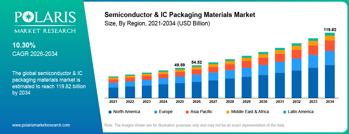
Global semiconductor & IC packaging materials market size was valued at USD 49.59 billion in 2025. The market is anticipated to grow from USD 54.52 billion in 2026 to USD 119.82 billion by 2034, exhibiting the CAGR of 10.30% during the forecast period
Market Statistics
Semiconductor & IC packaging Materials Market Key Takeaways
- Asia Pacific dominated the market with a 41.7% revenue share in 2025. The market leadership was attributed to strong semiconductor manufacturing and packaging activities.
- North America is anticipated to grow at a CAGR of 9.8% during 2026–2034. The increased investment in semiconductor research and advanced packaging is expected to boost the market.
- Organic substrates accounted for 27.9% of revenue in 2025. Their good thermal performance and lower cost made them the leading material.
- The QFN packaging segment is projected to grow at a CAGR of 10.4% during 2026–2034. Its use is increasing as it has compact design and efficient heat management property.
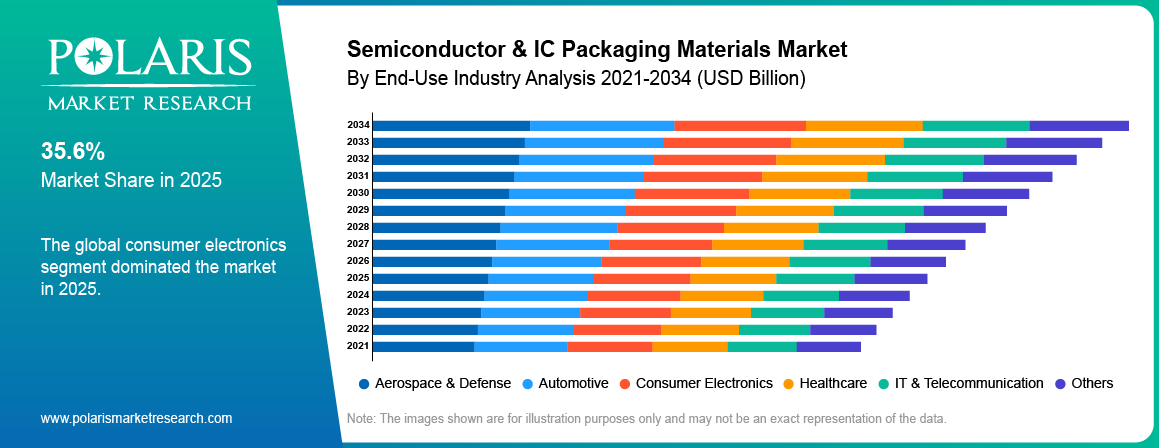
- Consumer electronics held 35.6% of market revenue in 2025. Higher demand for smartphones, laptops, and wearable devices supported the segment.
- The automotive segment is expected to register a CAGR of 11.2% during 2026–2034. Demand is boosted by increasing semiconductor use in electric and connected vehicles.
Note: Figures and projections outlined in this report are the result of Polaris Market Research’s proprietary analytical processes, grounded in the latest available datasets and market observations.
What Are Semiconductor & IC Packaging Materials? Definition, Functions & Material Types
Semiconductor & IC packaging materials are used to protect, support and connect semiconductor chips after their manufacturing. They facilitate electrical connections, dissipate heat and protect chips from moisture, dust and mechanical damage. These materials are the key to improving chip performance, reliability and durability. These are widely used in smartphones, computers, automotive electronics, AI processors, communication equipment and other electronic devices.
How Do Semiconductor Packaging Materials Work? Die Attach, Interconnect, Encapsulation, Substrate & Thermal Management
The process starts with the fabrication of a semiconductor wafer that contains multiple chips. The individual chips are then separated from the wafer. The individual chips are then attached to a package or a substrate with die-attach materials. The electrical connections needed for the operation of the chip are made with bonding wires or other sophisticated interconnects.
The encapsulation materials are then used to cover and protect the chip from moisture, dust and physical damage. The thermal interface materials are applied to remove the heat from chip to ensure the stable operation. The packaged semiconductor chips are integrated into the electronic products after the packaging process. These are used in smartphones, computers, automotive systems, communication devices and industrial equipment.
AI & HPC Impact on Semiconductor Packaging Materials: Chiplets, 2.5D/3D, Thermal Management & Substrates
- AI is increasing demand for advanced semiconductor packaging materials for high-performance AI chips.
- AI is driving the adoption of chiplet and 2.5D/3D packaging technologies.
- AI in manufacturing improves quality and reduces production defects.
- Demand for advanced packaging materials to be boosted by AI data center growth.
To Understand More About this Research:Download Sample Report
Semiconductor Packaging Materials Trends: AI/HPC, Chiplets, Hybrid Bonding & Advanced Substrates
Semiconductor and IC (Integrated Circuit) packaging materials are essential components used in the assembly and packaging of semiconductor devices, such as microchips and integrated circuits. These materials serve multiple purposes, including protecting the delicate semiconductor components from environmental factors such as moisture, dust, and physical damage, as well as providing electrical insulation and thermal management.
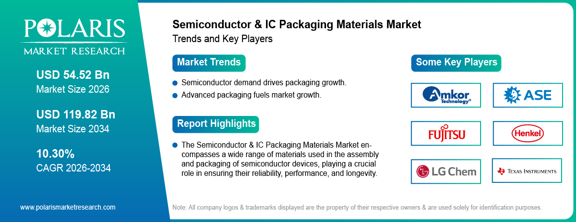
The Semiconductor & IC Packaging Materials Market encompasses a wide range of materials used in the assembly and packaging of semiconductor devices, playing a crucial role in ensuring their reliability, performance, and longevity. The market is driven by the rapid proliferation of semiconductor devices in various applications such as consumer electronics, automotive, telecommunications, and industrial automation. With the continuous evolution of semiconductor technology and the increasing demand for smaller, faster, and more powerful electronic devices, the need for advanced packaging materials with superior properties such as thermal conductivity, electrical insulation, and reliability is on the rise.
The market trends toward the growing demand for miniaturization and integration of semiconductor devices are leading to the development of advanced packaging solutions that offer higher performance and functionality in smaller form factors. Also, the increasing adoption of heterogeneous integration, which involves combining different semiconductor materials and technologies in a single package, is driving the need for versatile packaging materials capable of accommodating diverse device architectures.
The increasing demand for semiconductor devices across diverse end-use industries, including consumer electronics, automotive, healthcare, and telecommunications, is fueling demand for packaging materials to support the production of these devices. Similarly, technological advancements in semiconductor packaging techniques, such as flip-chip, wafer-level packaging, and through-silicon vias (TSVs), are driving the need for specialized packaging materials optimized for these advanced packaging processes. However, the market is hindered by the increasing cost and complexity of developing and manufacturing advanced packaging materials with superior properties and performance characteristics.
Traditional vs Advanced Semiconductor Packaging: Density, Thermal Performance, Chiplets & Materials
| Feature | Traditional Packaging | Advanced Packaging |
| Integration Density | Moderate | High |
| Performance | Standard | Enhanced |
| Power Efficiency | Moderate | High |
| AI/HPC Compatibility | Limited | Excellent |
| Miniaturization | Moderate | Advanced |
Source: Polaris Market Research Analysis
What are the market drivers driving the demand for the market?
The increasing demand for semiconductor devices is driving semiconductor & IC packaging materials market growth.
The increasing demand for semiconductor devices is significantly driving the market as industries such as consumer electronics, automotive, telecommunications, and industrial automation continue to integrate semiconductor technology into their products. The demand for packaging materials to support the production of these devices rises correspondingly. Semiconductor packaging materials play a crucial role in ensuring the performance and longevity of semiconductor devices by protecting them from environmental factors, providing electrical insulation, and managing thermal properties.
Also, as the demand for electronic devices with higher performance, increased functionality, and smaller form factors continues to grow, there is a parallel need for advanced packaging materials capable of meeting these evolving requirements. This market trend is expected to drive sustained semiconductor & IC packaging materials market growth as semiconductor manufacturers strive to meet the increasing demand for semiconductor devices across various industries.
Advanced Packaging Materials for FOWLP, 2.5D/3D, SiP & Hybrid Bonding
Advanced semiconductor packaging is becoming more widely used as chips become smaller, faster, and more complex. Technologies such as Fan-Out Wafer-Level Packaging (FOWLP), 2.5D Packaging, 3D IC Packaging, System-in-Package (SiP), Chiplet Integration, and Hybrid Bonding improve chip performance, increase integration density, and enhance power efficiency. These packaging approaches also enable AI processors, high-performance computing, automotive electronics and other advanced applications.
Chiplet Packaging Materials: Substrates, Underfills, RDL Dielectrics & Thermal Materials
As chip manufacturers look for better performance and more efficient production chiplet-based semiconductor design is gaining popularity. Instead of building a single large chip, multiple smaller chiplets are combined into one package. This technique lowers manufacturing costs, increases design flexibility, and reduces development time. Advanced packaging materials provide reliable chiplet connections and better heat management. The growing demand for AI, data centers, and high-performance computing is driving the adoption of chiplet-based designs.
Trends in Heterogeneous Integration
Semiconductor manufacturers are increasingly integrating logic chips, memory, sensors, RF devices and accelerators into a single package. This improves device performance, saves space, and adds more functions. As heterogeneous integration increases, so does the demand for advanced semiconductor packaging materials.
Which factor is restraining the demand for Semiconductor & IC Packaging Materials?
The cost and complexity of advanced materials are hindering the semiconductor & IC packaging materials market growth.
Developing and manufacturing advanced packaging materials with superior properties and performance characteristics incur significant costs and require intricate processes. The complexity of these materials often translates into higher production expenses, making them less accessible to semiconductor manufacturers, particularly smaller players or those operating in cost-sensitive markets. Also, the intricacies of advanced materials require specialized equipment, expertise, and quality control measures, further adding to the overall complexity and cost of production. These factors act as barriers to adoption, limiting the widespread use of advanced packaging materials and hindering semiconductor & IC packaging materials market growth.
Semiconductor & IC Packaging Materials Market Segmentation Analysis
The market is primarily segmented based on type, packaging technology, end-use industry, and region.
| By Type | By Packaging Technology | By End-Use Industry | By Region |
|
|
|
|
Source: Polaris Market Research Analysis
Semiconductor Packaging Materials by Type
Based on type analysis, the market has been segmented on the basis of bonding wires, ceramic packages, die-attach materials, encapsulation resins, lead frames, Organic substrates accounted for 27.9% of revenue in 2025, the organic substrate segment asserted its dominance in the market since they are made from materials such as laminate or fiberglass-reinforced epoxy resin, which are widely used in semiconductor packaging due to their excellent electrical insulation properties, thermal performance, and cost-effectiveness. These substrates serve as the foundation for mounting and interconnecting semiconductor chips, providing mechanical support and electrical connectivity within electronic devices.
Organic substrates also offer advantages such as lightweight, flexibility, and compatibility with high-density interconnect (HDI) technologies, making them well-suited for miniaturized and high-performance electronic applications. The increasing demand for compact and lightweight electronic devices, coupled with the growing adoption of advanced packaging techniques such as FOWLP and system-in-package, further drives the demand for organic substrates in the global market.
Semiconductor & IC Packaging Materials Market by End-Use Industry
Based on application category analysis, the market has been segmented on the basis of aerospace & defense, automotive, consumer electronics, healthcare, IT & telecommunication, and others. Consumer electronics held 35.6% of market revenue in 2025 accounted for the highest Semiconductor & IC Packaging Materials market share since consumer electronics, including smartphones, tablets, laptops, wearable devices, and home appliances, have witnessed exponential growth in demand. As consumer electronics become more sophisticated, compact, and feature-rich, the demand for semiconductor devices with higher performance, reliability, and miniaturization increases correspondingly.
Semiconductor packaging materials play a critical role in enabling the production of advanced semiconductor devices used in consumer electronics, providing essential functions such as electrical insulation, thermal management, and mechanical support. Also, the rapid pace of innovation and product development in the consumer electronics industry necessitates continuous advancements in semiconductor packaging materials to meet evolving performance requirements and cost considerations. As a result, the consumer electronics segment emerges as a dominant segment of the global market.
Common Applications of Semiconductor Packaging Materials
| Application | Purpose |
| Smartphone Processors | Protect chips and help smartphones run smoothly |
| AI Accelerators | Support high-speed AI processing and computing tasks |
| Graphics Processing Units (GPUs) | Help manage heat during graphics processing |
| Automotive Electronics | Used in vehicle control, safety, and infotainment systems |
| Electric Vehicle Systems | Support battery systems and power management |
| Data Center Chips | Help servers deliver stable and reliable performance |
| IoT Devices | Help power compact and connected smart devices |
| Medical Electronics | Support medical imaging and patient monitoring equipment |
| Telecommunications Infrastructure | Used in 5G networks and communication systems |
| Consumer Electronics Devices | Used in laptops, tablets, wearables, and home electronics |
Source: Polaris Market Research Analysis
Semiconductor & IC Packaging Materials Market by Region
Asia Pacific
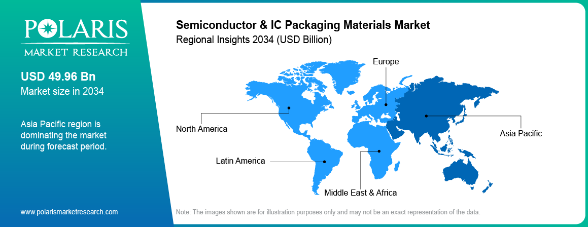
Asia Pacific dominated the market with a 41.7% revenue share in 2025. With countries like Japan, China, Taiwan, South Korea, and Singapore, the region boasts of several electronics manufacturing hubs that have a comprehensive presence of foundries, packaging facilities, equipment suppliers, and research institutions, creating an integrated and highly competitive market environment that fosters continuous innovation and technological advancement. This integration is particularly evident in countries like South Korea and Japan, which are renowned for their leadership in semiconductor research and manufacturing.
North America
North America is anticipated to grow at a CAGR of 9.8% during 2026–2034 growth due to the presence of major players, coupled with significant investments in research and development, innovation, and technological advancements, which positions North America as a hub for semiconductor packaging materials development and production. Also, the region's strong focus on emerging technologies such as artificial intelligence, the Internet of Things, and 5G connectivity drives demand for advanced semiconductor devices with higher performance, reliability, and efficiency, further boosting the demand for innovative packaging materials.
Semiconductor Packaging Materials Competitive Landscape & Leading Suppliers
The competitive landscape for the market is characterized by intense competition among key players competing for market share and technological leadership. Major players in the market include prominent materials manufacturers such as Henkel AG & Co. KGaA, LG Chem, Siliconware Precision Industries Co., Ltd., and Kyocera Corporation, among others. These companies offer a diverse portfolio of packaging materials tailored to meet the stringent requirements of semiconductor packaging applications, including substrates, encapsulants, bonding wires, and thermal interface materials. Moreover, there is a growing presence of niche players and startups specializing in innovative materials and technologies to address specific market needs and emerging trends.
Some of the major players operating in the global market include:
- Amkor Technology
- ASE
- Fujitsu Semiconductor Memory Solution Limited
- Henkel AG & Co. KGaA
- IBIDEN
- KYOCERA Corporation
- LG Chem
- Powertech Technology Inc.
- Siliconware Precision Industries Co., Ltd.
- Texas Instruments Incorporated
Semiconductor Packaging Materials Market Challenges: Cost, Thermal Management, Warpage, Reliability & Supply Risk
The semiconductor & IC packaging materials market faces several challenges. High R & D costs are associated with new materials. Advanced packaging processes are complex and need specialized equipment. With more powerful chips heat management is becoming more challenging. Supply chain issues can impact the availability of raw material. Packaging materials have to meet strict quality standards prior to usage. Advanced packaging also increases production costs. Particularly for smaller manufacturers these challenges can slow market growth and make expansion difficult.
Semiconductor Packaging Materials Market Developments: Advanced Substrates, EMC, Dielectrics, Underfills & Thermal Materials
- May 2026: Kyocera launched a multilayer ceramic core substrate for AI chip packaging. It allows more wiring in a smaller space and helps reduce bending of the package. It is mainly used in AI chips and data center systems.(Source: europe.kyocera.com)
- January 2026: SP Samhwa started volume production of a new epoxy molding compound (EMC) to be used in semiconductor packaging. The material is used in chip packages for mobile devices and protects the semiconductor chips from damage, allowing them to work reliably.(Source: www.mk.co.kr)
- In February 2025, ASE Technology Holding inaugurated its largest overseas facility in Penang, Malaysia. The launch aims to expand operations in robotics and AI, support supply chain realignment, and reinforce its position as the world’s largest chip assembly and testing provider.
- In February 2025, Resonac outlined plans for acquisitions following post-restructuring measures after lowering borrowings, with the objective of strengthening its market position amid intense competition.
- In January 2025, GlobalFoundries (GF) announced an investment of USD 575 million to build an advanced microchip packaging and photonics center in Malta, New York, supported by federal and state funding.
Semiconductor & IC Packaging Materials Market Future Outlook: AI/HPC, Chiplets, 3D Integration & Advanced Thermal Materials
The semiconductor & IC packaging materials market is expected to grow steadily in the coming years. Increasing demand for AI, high-performance computing, electric vehicles, 5G networks, and consumer electronics will drive market growth. The market for advanced packaging technologies such as chiplets, heterogeneous integration, hybrid bonding and 3D IC packaging will also boost the demand for specialized materials. The market growth is expected to be propelled by the ongoing investments in packaging facilities and local semiconductor supply chains.
Semiconductor & IC Packaging Materials Market Report Coverage, Scope & Competitive Analysis
The Semiconductor & IC Packaging Materials market report emphasizes key regions across the globe to provide a better understanding of the product to the users. Also, the report provides market insights into recent developments and trends and analyzes the technologies that are gaining traction around the globe. Furthermore, the report covers an in-depth qualitative analysis pertaining to various paradigm shifts associated with the transformation of these solutions.
The report provides a detailed analysis of the market while focusing on various key aspects such as competitive analysis, type, packaging technology, end-use industry, and their futuristic growth opportunities.
Semiconductor & IC Packaging Materials Market Report Scope, Segmentation & Forecast Coverage
| Report Attributes | Details |
| Market size value in 2025 | USD 49.59 billion |
| Market size value in 2026 | USD 54.52 billion |
| Revenue Forecast in 2034 | USD 119.82 billion |
| CAGR | 10.30% from 2026 – 2034 |
| Base year | 2025 |
| Historical data | 2021 – 2024 |
| Forecast period | 2026 – 2034 |
| Quantitative units | Revenue in USD billion and CAGR from 2026 to 2034 |
| Segments Covered | By Type, By Packaging Technology, By End-Use Industry, By Region |
| Regional scope | North America, Europe, Asia Pacific, Latin America; Middle East & Africa |
| Customization | Report customization as per your requirements with respect to countries, regions, and segmentation. |
Source: Polaris Market Research Analysis
Semiconductor & IC Packaging Materials Market FAQ's
The Semiconductor & IC Packaging Materials Market report covering key segments are type, packaging technology, end-use industry, and region.
Semiconductor & IC Packaging Materials Market Size Worth USD 119.82 Billion by 2034
Semiconductor & IC packaging materials market exhibiting the CAGR of 10.30% during the forecast period
Asia Pacific dominated the market, accounting for a 41.7% revenue share in 2025.
key driving factors in Semiconductor & IC Packaging Materials Market are increasing demand for semiconductor devices
Semiconductor packaging materials protect and support semiconductor chips. Semiconductor packaging materials also connect the chips to electronic devices.
They guard chips from heat, moisture and damage. They improve and extend the life of chips.
Typical materials are organic substrates, bonding wires, encapsulation resins, solder balls and leadframes. Each material has a different function.
Advanced semiconductor packaging connects chips in more efficient ways. It aids in improving performance, while reducing the size of electronic devices.
They help to remove heat and provide stable electrical connections, which improves chip reliability and overall performance.
Download Sample Report of Semiconductor & IC Packaging Materials Market
Please fill out the form to request a customized copy of the research report.


