
Semiconductor Assembly And Packaging Equipment Market Size, Share, Analysis & Forecast, 2025-2034
REPORT DETAILS
REPORT DETAILS
ABOUT THIS REPORT
Market Statistics
Overview
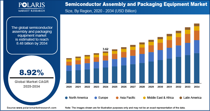
The global semiconductor assembly and packaging equipment market size was valued at USD 3.62 billion in 2024, growing at a CAGR of 8.92% from 2025 to 2034. The market is growing due to rising demand for advanced packaging solutions, growing investments in automation/technological advancements, and rapid adoption of AI, IoT and 5G devices requiring high-performance chips.
Key Insights
- The bonding equipment segment accounted for largest revenue share in 2024 due to its critical role in enabling the miniaturization and performance enhancement of semiconductor devices.
- The wafer level packaging (WLP) equipment segment dominated the revenue share in 2024 due to its capability to support compact, high-performance semiconductor designs.
- The OSAT segment is expected to witness the fastest growth during the forecast period, driven by the increasing trend of fabless semiconductor design and the outsourcing of back-end processes.
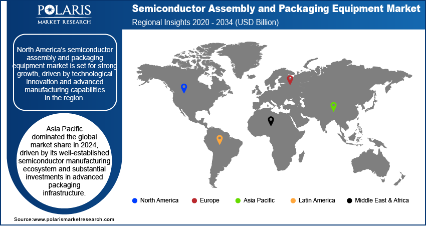
- The North America semiconductor assembly and packaging equipment market is expected to witness significant growth during the forecast period driven by the region’s strong focus on technological innovation and advanced manufacturing.
- The U.S. held a substantial market share in North America in 2024 due to its strong presence of leading semiconductor manufacturers and advanced R&D infrastructure.
- Asia Pacific dominated the global market share in 2024, driven by its well-established semiconductor manufacturing ecosystem and substantial investments in advanced packaging infrastructure.
- The market in India is expanding due to increasing government initiatives aimed at developing a localized semiconductor ecosystem.
Industry Dynamics
- Rising investments in automation and advanced packaging solutions are boosting efficiency, precision, and production speed, creating growth potential for semiconductor assembly and packaging equipment manufacturers.
- The rapid expansion of AI, IoT, and 5G devices is increasing demand for high-performance, power-efficient chips, pushing the need for innovative packaging solutions beyond traditional methods.
- Developing advanced packaging technologies requires massive R&D investments, creating profit margins for smaller players and slowing time-to-market for innovating solutions.
- The shift toward chiplet-based designs and 3D packaging opens new revenue streams, as companies compete to meet the need for faster, more compact, and power-efficient semiconductor solutions.
Market Statistics
- 2024 Market Size: USD 3.62 billion
- 2034 Projected Market Size: USD 8.48 billion
- CAGR (2025–2034): 8.92%
- Asia Pacific: Largest market in 2024
To Understand More About this Research: Download Sample Report
Semiconductor assembly and packaging equipment refers to the machinery and tools used to assemble, interconnect, and encapsulate semiconductor devices, preparing them for final integration into electronic products. The market is witnessing notable growth driven by the surging demand for advanced packaging technologies. Advanced packaging, such as 2.5D/3D ICs, fan-out wafer-level packaging, and system-in-package, has become essential to ensure higher performance, better thermal management, and increased functionality as chip designs become more complex and miniaturized. In October 2024, DELO developed a new approach for fan-out wafer-level packaging, which replaces heat-cured materials with UV-curable alternatives, cutting warpage by 50% and die shift greatly. The innovation reduces viscosity to 35,000 mPa·s (versus 800,000 mPa · s) and Young's modulus to 1 GPa, while reducing curing time and energy consumption. This technological shift is driving semiconductor manufacturers to invest heavily in advanced assembly and packaging equipment to maintain a competitive edge and meet the performance requirements of next-generation applications, such as AI, 5G, and high-performance computing.
The increasing support from governments worldwide, through strategic initiatives and localization efforts aimed at strengthening domestic semiconductor manufacturing capabilities, further boosts growth opportunities. According to a July 2024 report by the Ministry of Electronics & IT, India approved USD 9.1 billion for the Semicon India programme to boost semiconductor and display manufacturing. The scheme offers financial incentives for chip production, display fabrication, and the development of the design ecosystem, thereby strengthening India's electronics manufacturing capabilities. Many countries are implementing policies that incentivize local production and reduce reliance on foreign supply chains, particularly in response to recent global disruptions. These government-led programs are encouraging the establishment of new semiconductor fabless and packaging facilities, creating demand for state-of-the-art assembly and packaging equipment. This localization push is accelerating the adoption of advanced equipment to meet both national and global supply needs.
Drivers and Opportunities
Increasing Investments in Advancement and Automation: Manufacturers aim to enhance production efficiency, precision, and throughput. In April 2025, Applied Materials finalized its acquisition of Besi and expanded its partnership to co-develop the first fully integrated hybrid bonding solution. This copper-to-copper chip connection technology enhances performance, reduces power consumption, and lowers costs in advanced semiconductor packaging. Automated systems are becoming increasingly essential for managing complex processes such as wafer handling, die bonding, and inspection with the continuous push for smaller, faster, and more powerful chips. Advanced automation reduces human error, ensures consistent quality, and supports high-volume manufacturing with greater scalability. These improvements reduce operational costs over time and also enable manufacturers to keep pace with rapid innovation cycles and evolving end user demands in consumer electronics, automotive, and industrial applications. Thus, increasing investments in advancement and automation is driving growth opportunities.
Rising Adoption of AI, IoT, and 5G-Enabled Devices: The increasing adoption of AI, IoT, and 5G-enabled devices is driving the demand for semiconductor assembly and packaging equipment. According to a March 2025 report by the Ministry of Commerce and Industry, India's 5G device ecosystem experienced rapid growth in 2024, with the number of active devices doubling to 271 million. The trend continues, with 90% of smartphone replacements in 2025 expected to be 5G-capable. These technologies require highly integrated, high-performance chips with efficient power management and compact form factors, pushing the boundaries of traditional packaging. As a result, there is a growing need for advanced equipment capable of supporting heterogeneous integration, multi-chip modules, and other refined packaging architectures. The expansion of connected devices and intelligent systems further boosts the demand for reliable and high-throughput packaging solutions, thereby accelerating investments in next-generation assembly and packaging tools across the semiconductor value chain.
Segmental Insights
Product Analysis
Based on product, the segmentation includes dicing equipment, bonding equipment, packaging equipment, and others. The bonding equipment segment accounted for the largest revenue share in 2024 due to its critical role in enabling the miniaturization and performance enhancement of semiconductor devices. Precision bonding technologies, such as wire bonding, flip-chip bonding, and die attach, have become essential for high-density integration as semiconductor packages become increasingly complex and multilayered. The growing demand for advanced electronic devices across various sectors, such as consumer electronics, automotive, and industrial automation, has increased the need for reliable and high-throughput bonding equipment. Additionally, innovations in bonding techniques are supporting newer packaging architectures, reinforcing the segment’s dominant position.
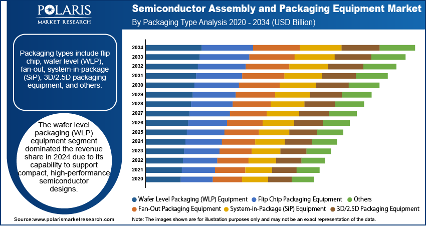
Packaging Type Analysis
In terms of packaging type, the segmentation includes flip chip packaging equipment, wafer level packaging (WLP) equipment, fan-out packaging equipment, system-in-package (SiP) equipment, 3D/2.5D packaging equipment, and others. The wafer level packaging (WLP) equipment segment dominated the revenue share in 2024 due to its capability to support compact, high-performance semiconductor designs. WLP enables the packaging of chips at the wafer level, improving electrical performance, reducing form factor, and minimizing manufacturing costs. The industry is shifting increasingly toward fan-in and fan-out WLP to meet the growing demand for smaller and more efficient components, with the expansion of mobile devices, wearables, and IoT applications. The scalability, cost-effectiveness, and high-yield characteristics of WLP have made it a preferred packaging solution, driving strong adoption of WLP equipment across manufacturing facilities.
End Use Analysis
The segmentation, based on end use, includes IDMs (integrated device manufacturers) and OSAT (outsourced semiconductor assembly and test). The OSAT (outsourced semiconductor assembly and test) segment is expected to witness fastest growth during the forecast period, driven by the increasing trend of fabless semiconductor design and the outsourcing of back-end processes. Chipmakers are increasingly relying on OSAT providers for cost-effective, scalable, and technologically advanced assembly and testing services as they focus on core competencies such as design and innovation. OSAT players are rapidly investing in innovative packaging technologies and equipment to meet the complex requirements of AI, automotive, and high-performance computing applications. This outsourcing model enhances operational flexibility, allowing for the rapid adoption of advanced packaging tools and contributing to the segment’s accelerated growth.
Regional Analysis
The North America semiconductor assembly and packaging equipment market is expected to witness significant growth during the forecast period, driven by the region’s strong focus on technological innovation and advanced manufacturing. Continued investments in next-generation semiconductors, coupled with growing demand for high-performance computing, AI, and telecommunications infrastructure, are driving the need for refined packaging solutions. Furthermore, the presence of major industry players and research institutions, along with supportive policy initiatives aimed at strengthening domestic chip production, is boosting equipment demand and establishing North America as a hub for semiconductor advancement.
U.S. Semiconductor Assembly and Packaging Equipment Market Insights
The U.S. held a substantial share in North America semiconductor assembly and packaging equipment landscape in 2024 due to its strong presence of leading semiconductor manufacturers and advanced R&D infrastructure. The country’s focus on high-performance computing, aerospace electronics, and AI-driven applications has driven continuous investments in advanced packaging technologies. Additionally, supportive national policies and strategic initiatives aimed at boosting domestic chip production have strengthened demand for equipment across major facilities.
Asia Pacific Semiconductor Assembly and Packaging Equipment Market Trends
The market in Asia Pacific dominated the global share in 2024, driven by its well-established semiconductor manufacturing ecosystem and substantial investments in advanced packaging infrastructure. The region is home to major foundries, OSAT providers, and component suppliers, which collectively fuel demand for high-volume, cost-effective assembly and packaging equipment. Additionally, rapid digital transformation, regional government support for semiconductor self-reliance, and increasing demand for consumer electronics are driving capacity expansions and technological upgrades. According to a July 2024 NITI Aayog report, India's electronics sector reached USD 155 billion in FY23, with production doubling to USD 101 billion. Mobile phones alone accounted for 43% of this output, with 99% manufactured domestically, indicating the region's growing focus on localized production and the increasing demand for semiconductor packaging equipment. These factors have solidified Asia Pacific’s leadership in semiconductor equipment deployment and market dominance.
India Semiconductor Assembly and Packaging Equipment Market Overview
The market in India is expanding due to increasing government-backed initiatives aimed at developing a localized semiconductor ecosystem. Growing interest from global players, rising domestic electronics consumption, and emerging investments in semiconductor fabs are contributing to the demand for modern assembly and packaging tools. India’s focus on becoming a manufacturing and design hub is further accelerating the adoption of advanced equipment in the back-end semiconductor supply chain.
Europe Semiconductor Assembly and Packaging Equipment Market Outlook
The semiconductor assembly and packaging equipment industry in Europe is projected to witness fastest growth during the forecast period driven by increasing regional efforts to enhance semiconductor dominance and develop advanced chip manufacturing capabilities. Europe is promoting innovation in semiconductor packaging technologies, particularly for automotive, industrial, and telecom applications, as part of broader strategic initiatives. The push toward developing high-performance, energy-efficient electronic components is encouraging investments in modern assembly and packaging tools. For instance, in March 2024, Silicon Box announced a USD 3.6 billion investment in Northern Italy to build Europe’s first advanced chiplet-based packaging facility. The plant will meet rising demand for next-gen semiconductor packaging, with full-scale production expected by 2028. This momentum, supported by public-private collaborations and research and development (R&D) funding, is expected to accelerate expansion across the region.
Germany Semiconductor Assembly and Packaging Equipment Market
The market growth in Germany is driven by its strong industrial base and leadership in automotive electronics, which demand high-reliability and precision semiconductor components. The country’s focus on integrating advanced technologies, such as autonomous driving and Industry 4.0, has increased the need for refined chip packaging solutions. Furthermore, sustained investments in high-tech infrastructure and engineering excellence boost the adoption of next-generation semiconductor assembly and packaging equipment.
Key Players and Competitive Analysis
The semiconductor assembly and packaging equipment sector is experiencing intense competition, driven by strategic investments in both emerging and developed markets, as companies seek to capitalize on revenue opportunities. Major players are leveraging competitive intelligence and strategy to navigate economic and geopolitical shifts, while technological advancements in advanced packaging, such as chiplets and panel-level integration, are reshaping industry trends. Small and medium-sized businesses are gaining traction by focusing on niche, emerging market segments, while larger firms expand through strategic expansion, including partnerships and acquisitions. Supply chain disruptions and sustainable value chains remain critical challenges, prompting companies to optimize partner & customer ecosystems. Growth projections highlight latent demand in AI, IoT, and automotive applications, with region-wise market size variations influencing vendor strategies. Expert insights suggest that future development strategies must strike a balance between innovation and cost efficiency to maintain a competitive position in this rapidly evolving landscape.
A few major companies operating in the semiconductor assembly and packaging equipment industry include Applied Materials; ASM Pacific Technology; Besi; Disco Corporation; Kulicke & Soffa Industries, Inc. (K&S); Nikon Corporation; Plasma-Therm; Rudolph Technologies, Inc.; SCREEN Semiconductor Solutions Co., Ltd.; and SUSS MicroTec SE.
Key Players
- Applied Materials
- ASM Pacific Technology
- Besi
- Disco Corporation
- Kulicke & Soffa Industries, Inc. (K&S)
- Nikon Corporation
- Plasma-Therm
- Rudolph Technologies, Inc.
- SCREEN Semiconductor Solutions Co., Ltd.
- SUSS MicroTec SE
Semiconductor Assembly and Packaging Equipment Industry Developments
- March 2025: iSABers launched the world’s first C2W&W2W Dual-Mode Hybrid Bonding Equipment (SAB 82CWW Series). The technology enables flexible chip-to-wafer & wafer-to-wafer bonding in advanced packaging.
- February 2025: RRP Electronics collaborated with Deca Technologies to acquire advanced wafer-level packaging tech, including M-Series and Adaptive Patterning. This enhances India’s semiconductor capabilities with real-time optimization, 10 times faster throughput, and global competitiveness in chip manufacturing.
Semiconductor Assembly and Packaging Equipment Market Segmentation
By Product Outlook (Revenue, USD Billion, 2020–2034)
- Dicing Equipment
- Scriber
- Dicer
- Wafer Mounting Equipment
- Bonding Equipment
- Die Bonder
- Wire Bonder
- Others
- Packaging Equipment
- Molding Equipment
- Solder Plating Equipment
- Deflasher
- Others
- Others
By Packaging Type Outlook (Revenue, USD Billion, 2020–2034)
- Flip Chip Packaging Equipment
- Wafer Level Packaging (WLP) Equipment
- Fan-Out Packaging Equipment
- System-in-Package (SiP) Equipment
- 3D/2.5D Packaging Equipment
- Others
By End Use Outlook (Revenue, USD Billion, 2020–2034)
- IDMs (Integrated Device Manufacturers)
- OSAT (Outsourced Semiconductor Assembly and Test)
By Regional Outlook (Revenue, USD Billion, 2020–2034)
- North America
- U.S.
- Canada
- Europe
- Germany
- France
- UK
- Italy
- Spain
- Netherlands
- Russia
- Rest of Europe
- Asia Pacific
- China
- Japan
- India
- Malaysia
- South Korea
- Indonesia
- Australia
- Vietnam
- Rest of Asia Pacific
- Middle East & Africa
- Saudi Arabia
- UAE
- Israel
- South Africa
- Rest of Middle East & Africa
- Latin America
- Mexico
- Brazil
- Argentina
- Rest of Latin America
Semiconductor Assembly and Packaging Equipment Market Report Scope
| Report Attributes | Details |
| Market Size in 2024 | USD 3.62 Billion |
| Market Size in 2025 | USD 3.93 Billion |
| Revenue Forecast by 2034 | USD 8.48 Billion |
| CAGR | 8.92% from 2025 to 2034 |
| Base Year | 2024 |
| Historical Data | 2020–2023 |
| Forecast Period | 2025–2034 |
| Quantitative Units | Revenue in USD Billion and CAGR from 2025 to 2034 |
| Report Coverage | Revenue Forecast, Competitive Landscape, Growth Factors, and Industry Trends |
| Segments Covered |
|
| Regional Scope |
|
| Competitive Landscape |
|
| Report Format |
|
| Customization | Report customization as per your requirements with respect to countries, regions, and segmentation. |
FAQ's
The global market size was valued at USD 3.62 billion in 2024 and is projected to grow to USD 8.48 billion by 2034.
The global market is projected to register a CAGR of 8.92% during the forecast period.
Asia Pacific dominated the market in 2024.
A few of the key players in the market are Applied Materials; ASM Pacific Technology; Besi; Disco Corporation; Kulicke & Soffa Industries, Inc. (K&S); Nikon Corporation; Plasma-Therm; Rudolph Technologies, Inc.; SCREEN Semiconductor Solutions Co., Ltd.; and SUSS MicroTec SE.
The wafer level packaging (WLP) equipment segment dominated the revenue share in 2024.
The OSAT (outsourced semiconductor assembly and test) is expected to witness fastest growth during the forecast period.
Download Sample Report of Semiconductor Assembly And Packaging Equipment Market
Please fill out the form to request a customized copy of the research report.
