
Reports

U.S. Semiconductor Assembly And Packaging Equipment Market Size, Share, Trends Analysis - 2025-2034
REPORT DETAILS
REPORT DETAILS
ABOUT THIS REPORT
Market Statistics
Overview
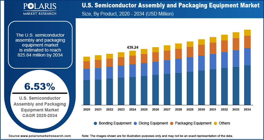
The U.S. semiconductor assembly and packaging equipment market size was valued at USD 439.24 million in 2024, growing at a CAGR of 6.53% from 2025 to 2034. The market is expanding due to the increasing need for refined packaging technologies, rising investments in automation and innovation, and the rapid adoption of AI, IoT and 5G applications demanding superior chip performance.
Key Insights
- The bonding equipment segment accounted for the largest revenue share in 2024, attributed to its pivotal role in supporting the miniaturization and performance optimization of semiconductor devices.
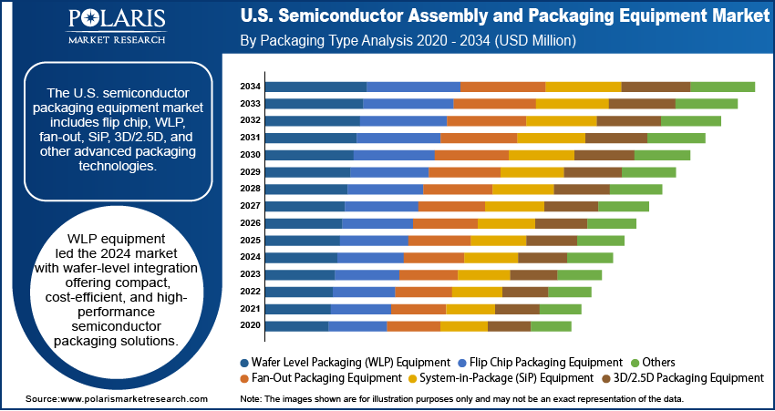
- The wafer level packaging (WLP) equipment segment dominated the revenue share in 2024 due to its ability to integrate chip-scale packaging processes directly at the wafer level, delivering superior electrical performance, compactness, and cost efficiency.
- The OSAT (outsourced semiconductor assembly and test) segment is expected to witness the fastest growth during the forecast period, primarily driven by the country's shift toward fabless semiconductor design models and the outsourcing of packaging and testing operations.
Industry Dynamics
- Growth opportunities are surging from advanced packaging demand, driven by rising needs for higher-performance, miniaturized devices.
- Government initiatives in the U.S. accelerate investments in innovative packaging infrastructure, including equipment upgrades and facility modernization.
- Developing advanced packaging technologies requires massive R&D investments, creating profit margins for smaller players and slowing time-to-market for advanced solutions.
- The shift toward chiplet-based designs and 3D packaging opens new revenue streams, as companies compete to meet the need for faster, more compact, and power-efficient semiconductor solutions.
Market Statistics
- 2024 Market Size: USD 439.24 million
- 2034 Projected Market Size: USD 825.84 million
- CAGR (2025–2034): 6.53%
To Understand More About this Research: Download Sample Report
Semiconductor assembly and packaging equipment refers to the machinery and tools used to assemble and encapsulate semiconductor devices, ensuring their functionality, durability, and connectivity in end-use applications. The U.S. semiconductor assembly and packaging equipment market is driven by increasing investments in technological advancements and automation. Manufacturers are prioritizing capital expenditures on advanced equipment that offers greater precision, yield optimization, and throughput as semiconductor packages become more compact and intricate. In April 2025, Applied Materials completed its acquisition of Besi to jointly create the industry's first fully integrated hybrid bonding solution. This copper-to-copper interconnect technology improves chip performance, decreases energy usage, and reduces packaging costs for advanced semiconductors. Automation is playing a critical role in reducing operational inefficiencies, improving process reliability, and enabling high-volume production, particularly as U.S. fabrication and OSAT providers focus on enhancing manufacturing competitiveness and reducing time-to-market.
The rising adoption of AI, IoT technology, and 5G-enabled devices is reshaping semiconductor demand patterns across the U.S. The integration of these technologies requires chips with higher performance, smaller form factors, and more complex package architectures, increasing the demand for advanced assembly and packaging solutions. The demand for high-density, multi-functional packaging equipment increases as end-use applications, ranging from autonomous vehicles and smart infrastructure to edge devices, become more refined. This shift is reinforcing the importance of next-generation assembly tools, driving market momentum, and encouraging domestic manufacturers to expand capabilities to meet evolving technological requirements.
Drivers & Opportunities
Surging Demand for Advanced Packaging Technologies: Advanced packaging technologies directly align with the shift toward higher-performance, miniaturized, and multifunctional devices. Higher-performing artificial intelligence, high-performance computing, and 5G applications require complex packaging formats, such as 2.5D/3D integration, system-in-package (SiP), and fan-out wafer-level packaging (FOWLP). In May 2025, Marvell Technology launched an advanced multi-die packaging platform for AI accelerators, enabling designs that are 2.8 times larger than those of single-die solutions. The innovation reduces power, improves yields, lowers costs, and offers an alternative to interposer-based approaches, helping hyperscalers overcome supply chain challenges in AI chip production. These innovations demand highly specialized equipment capable of handling increased interconnect densities, thermal management, and heterogeneous integration. Therefore, as U.S. manufacturers compete on performance and design innovation, the adoption of advanced packaging tools is becoming essential, fueling steady growth in equipment investment. Therefore, surging demand for advanced packaging technologies is driving growth of the U.S. semiconductor assembly and packaging equipment market.
Government Initiatives and Localization Efforts: Government initiatives and localization efforts play a pivotal role in driving the expansion opportunities. In November 2024, the U.S. U.S. Department of Commerce (DOC) plans to invest USD 300 million in advanced packaging research and development (R&D) to accelerate semiconductor innovation. The funding aims to boost next-gen packaging tech critical for chip manufacturing. Public policy is increasingly focused on incentivizing local manufacturing and reducing dependence on foreign supply chains, with a growing focus on strengthening domestic semiconductor capabilities. These efforts are promoting capital investments in state-of-the-art assembly and packaging infrastructure across the U.S., including equipment procurement and facility modernization. These initiatives enhance the implementation of advanced equipment and cultivate a favorable environment for sustained industry growth by promoting a more self-sufficient and robust semiconductor ecosystem.
Segmental Insights
Product Analysis
Based on product, the U.S. semiconductor assembly and packaging equipment market is segmented into dicing equipment, bonding equipment, packaging equipment, and others. The bonding equipment segment accounted for the largest revenue share in 2024 attributed to its pivotal role in supporting the miniaturization and performance optimization of semiconductor devices. Advanced bonding methods, such as wire bonding, flip-chip bonding, and die attach, are vital to enabling high-density, multilayered package architectures that align with the increasing complexity of U.S.-manufactured semiconductors. The rising demand for high-performance electronic products across domestic sectors, such as consumer electronics, automotive electronics, and industrial automation, has further fueled the adoption of high-precision and high-throughput bonding systems. Moreover, continual advancements in bonding technologies are enabling next-generation packaging formats, reinforcing the segment’s leadership within the U.S. market.
Packaging Type Analysis
In terms of packaging type, the U.S. semiconductor assembly and packaging equipment market segmentation includes flip chip packaging equipment, wafer level packaging (WLP) equipment, fan-out packaging equipment, system-in-package (SiP) equipment, 3D/2.5D packaging equipment, and others. The wafer level packaging (WLP) equipment segment dominated the revenue share in 2024 due to its ability to integrate chip-scale packaging processes directly at the wafer level, delivering superior electrical performance, compactness, and cost efficiency. The growing adoption of mobile devices, wearables, and Internet of Things (IoT) products across the U.S. is driving demand for fan-in and fan-out WLP technologies. Semiconductor manufacturers in the U.S. are increasingly investing in WLP equipment to meet consumer expectations for smaller, faster, and more energy-efficient devices. Its scalability and high production yields make WLP a strategic choice, accelerating its deployment across advanced packaging facilities nationwide.
End Use Analysis
The U.S. semiconductor assembly and packaging equipment market segmentation, based on end use, includes IDMs (integrated device manufacturers) and OSAT (outsourced semiconductor assembly and test). The OSAT (outsourced semiconductor assembly and test) is expected to witness the fastest growth during the forecast period, primarily driven by the country's shift toward fabless semiconductor design models and the outsourcing of packaging and testing operations. Leading U.S. chipmakers are prioritizing design and IP development while entrusting OSAT providers with the assembly and testing of increasingly complex semiconductor products. U.S.-based OSAT firms are scaling up investments in innovative packaging equipment to meet demand from high-growth sectors, such as artificial intelligence (AI), automotive electronics, and high-performance computing. This trend is enabling greater flexibility and speed to market, positioning OSAT providers as major contributors to the sector’s long-term expansion in the U.S.
Key Players and Competitive Analysis
Strategic investments, technological advancements, and shifts in economic and geopolitical conditions shape the U.S. semiconductor assembly and packaging equipment landscape. Major players dominate through competitive positioning, leveraging R&D in hybrid bonding and panel-level packaging to address latent demand and opportunities in AI and advanced computing. Industry trends indicate a shift toward heterogeneous integration, with growth projections tied to federal initiatives such as the CHIPS Act. Disruptions and trends in supply chains have accelerated localization, creating opportunities for domestic suppliers to expand their operations. Small and medium-sized businesses are gaining traction in niche segments, such as fan-out wafer-level packaging (FOWLP). At the same time, larger firms focus on sustainable value chains and partner & customer ecosystems. Expert’s insight highlights the need for future development strategies to counter China’s packaging dominance, with revenue growth relying on innovations in 3D IC integration and copper interconnect technologies. Vendor strategies now prioritize supply chain management and procurement resilience, with technological assessment guiding investments in automation and modular equipment designs.
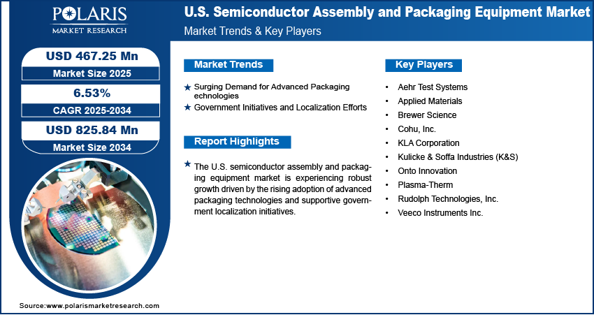
A few major companies operating in the U.S. semiconductor assembly and packaging equipment market include Aehr Test Systems; Applied Materials; Brewer Science; Cohu, Inc.; KLA Corporation; Kulicke & Soffa Industries (K&S); Onto Innovation; Plasma-Therm; Rudolph Technologies, Inc.; and Veeco Instruments Inc.
Key Players
- Aehr Test Systems
- Applied Materials
- Brewer Science
- Cohu, Inc.
- KLA Corporation
- Kulicke & Soffa Industries (K&S)
- Onto Innovation
- Plasma-Therm
- Rudolph Technologies, Inc.
- Veeco Instruments Inc.
U.S. Semiconductor Assembly and Packaging Equipment Industry Developments
- May 2025: Veeco Instruments received USD 35M+ of orders for its AP300 lithography systems from IDMs and OSATs, with planned deliveries in 2025. The systems support AI/HPC demand and advanced packaging (2.5D/3D, FOWLP).
- February 2025: RRP Electronics collaborated with Deca Technologies to acquire advanced wafer-level packaging tech, including M-Series and Adaptive Patterning. This enhances India’s semiconductor capabilities with real-time optimization, 10 times faster throughput, and competitiveness in chip manufacturing.
U.S. Semiconductor Assembly and Packaging Equipment Market Segmentation
By Product Outlook (Revenue, USD Million, 2020–2034)
- Dicing Equipment
- Scriber
- Dicer
- Wafer Mounting Equipment
- Bonding Equipment
- Die Bonder
- Wire Bonder
- Others
- Packaging Equipment
- Molding Equipment
- Solder Plating Equipment
- Deflasher
- Others
- Others
By Packaging Type Outlook (Revenue, USD Million, 2020–2034)
- Flip Chip Packaging Equipment
- Wafer Level Packaging (WLP) Equipment
- Fan-Out Packaging Equipment
- System-in-Package (SiP) Equipment
- 3D/2.5D Packaging Equipment
- Others
By End Use Outlook (Revenue, USD Million, 2020–2034)
- IDMs (Integrated Device Manufacturers)
- OSAT (Outsourced Semiconductor Assembly and Test)
U.S. Semiconductor Assembly and Packaging Equipment Market Report Scope
| Report Attributes | Details |
| Market Size in 2024 | USD 439.24 Million |
| Market Size in 2025 | USD 467.25 Million |
| Revenue Forecast by 2034 | USD 825.84 Million |
| CAGR | 6.53% from 2025 to 2034 |
| Base Year | 2024 |
| Historical Data | 2020–2023 |
| Forecast Period | 2025–2034 |
| Quantitative Units | Revenue in USD Million and CAGR from 2025 to 2034 |
| Report Coverage | Revenue Forecast, Competitive Landscape, Growth Factors, and Industry Trends |
| Segments Covered |
|
| Regional Scope |
|
| Competitive Landscape |
|
| Report Format |
|
| Customization | Report customization as per your requirements with respect to countries, regions, and segmentation. |
FAQ's
The market size was valued at USD 439.24 million in 2024 and is projected to grow to USD 825.84 million by 2034.
The market is projected to register a CAGR of 6.53% during the forecast period.
A few of the key players in the market are Aehr Test Systems; Applied Materials; Brewer Science; Cohu, Inc.; KLA Corporation; Kulicke & Soffa Industries (K&S); Onto Innovation; Plasma-Therm; Rudolph Technologies, Inc.; and Veeco Instruments Inc.
The wafer level packaging (WLP) equipment segment dominated the revenue share in 2024.
The OSAT (outsourced semiconductor assembly and test) segment is expected to witness the fastest growth during the forecast period.
Download Sample Report of U.S. Semiconductor Assembly And Packaging Equipment Market
Please fill out the form to request a customized copy of the research report.
