
Chiplets Market Size, Share, Trends & Forecast, 2026–2034
REPORT DETAILS
Chiplets Market Summary
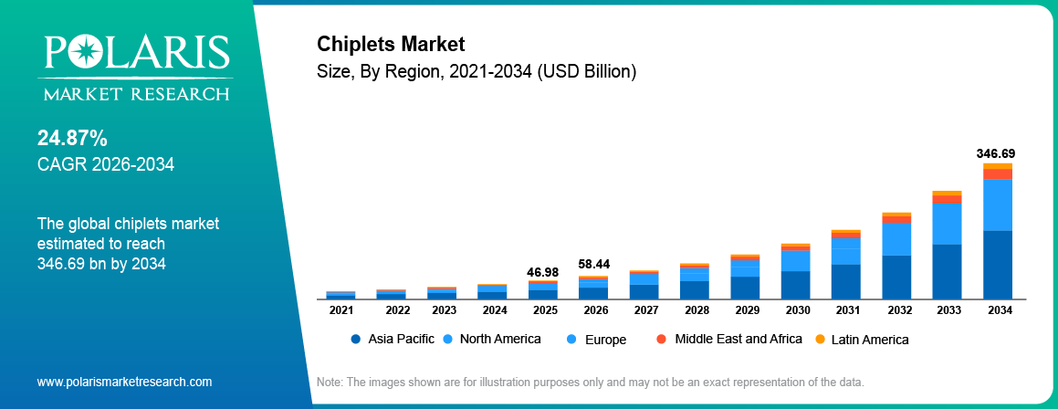
Chiplet market size was valued at USD 46.98 billion in 2025. The market is expected to grow at a CAGR of 24.87% from 2026 to 2034. The chiplets market growth is attributed to the rising demand for AI, HPC, data centers, and advanced semiconductor packaging.
Market Statistics
Key Takeaways
- Asia Pacific led the market with an 39.67% share in 2025. The dominance is supported by
- its strong semiconductor and advanced packaging ecosystem.
- The market in North America is expected to register the highest CAGR at 26.67% during the forecast period. The growth is attributed to the rising AI, HPC, and data center investments.
- The CPU segment led the market with 34.68% share in 2025. It is attributed to the rising adoption of modular processor design across PCs, servers, and data centers.
- The 2.5D/3D technology captured the major market share of 37.68% in 2025, due to its high density and performance.
- The consumer electronics segment held the largest revenue share of 27.68% in 2025. Rising demand for thinner and lighter designs of portable laptops and ultrabooks drives the segmental growth.
Note: Figures and projections outlined in this report are the result of Polaris Market Research’s proprietary analytical processes, grounded in the latest available datasets and market observations.
What are Chiplets?
Chiplets refer to small semiconducting devices that are purpose-built and assembled into one chip to construct advanced computing solutions. Chiplets allocate functions to different dies and link them using 2.5D/3D integration and System-in-Package (SiP) techniques.
Chiplets technology has gained prominence due to rising costs and complexity associated with large monolithic chips. It allows chipmakers to employ various process nodes, leverage IP, enhance yield, and develop more flexible processors.
The demand for chiplets has been fueled by increasing use of AI, high-performance computing (HPC), hyperscale data centers, advanced networking, and HBM. Chiplets have also found applications in the automotive, industrial automation, consumer electronics, and aerospace & defense sectors.
Chiplet integration is heavily dependent on advanced packaging. Packaging techniques like TSMC's 3DFabric, Intel's Foveros and EMIB, Samsung's heterogeneous integration, and ASE's advanced packaging solutions help integrate multiple dies, HBM, and other computing functions.
How do Chiplets Work
The chiplet design technique involves breaking down the semiconductor device into smaller dies, where each chiplet would be responsible for performing different functions like processing, memory, AI acceleration, or I/O. The dies are fabricated independently and assembled into a chiplet package with high-speed die to die interconnect.
The typical process includes:
- Design: Partition the system into functional chiplets.
- Fabrication: Fabricate the chiplets by using appropriate process nodes.
- Testing: Test the dies prior to packaging.
- Packaging: Package the chiplets using 2.5D, 3D, SiP, or fan-out techniques.
- Interconnection: Facilitate high-speed interconnects between chiplets.
- Validation: Verification: Validate the entire package in terms of its performance, thermals, behavior, and reliability.
The above method allows for heterogeneous integration, where different chiplets, process nodes, and functionalities coexist in a single package.
Chiplets vs Monolithic Chips
Chiplets do not eliminate monolithic chips. Instead, they provide an alternative architecture for increasingly complex semiconductor designs where integrating every function on a single die becomes less practical.
| Feature | Chiplets | Monolithic Chips |
| Manufacturing Cost | Lower | Higher |
| Yield Rate | Higher | Lower |
| Scalability | Excellent | Limited |
| Design Flexibility | High | Moderate |
| Time to Market | Faster | Slower |
| Packaging Complexity | Higher | Lower |
Source: Polaris Market Research Analysis
Market Dynamics
Drivers: Advantages of Chiplets Over Monolithic Design
Chiplets are smaller functional units made up of parts of an integrated circuit that eliminates the need of creation of single monolithic chips. The combination of different chiplets having specific functionalities, such as memory, processors, and input/output components allows designers to create an efficient and highly customized system. Thus, the chiplet technology is considered as the future of semiconductor design. Moreover, benefits such as modular approach to chip design, parallel development of different components, reduction in manufacturing costs, and improvement in yield rates are expected to fuel the overall chiplets market during the forecast period.
Driver: Growing Use of High-Performance Computing
The ability to analyze data and carry out complex calculations at high speeds is known as high performance computing (HPC). There is a rising adoption of HPC across sectors. For instance, in September 2026, HIVE’s BUZZ HPC partnered with ProCogia to deploy AI workloads on Canadian sovereign infrastructure, supporting scalable AI compute for enterprises and SMBs. With the utilization of chiplet-based technology, HPCs allow for the efficient integration of specialized processing units, accelerators, and memory. The growing need to design powerful chips and increasing adoption of HPCs in various fields such as finance, research, weather forecasting, manufacturing, pharmaceuticals, energy, government, automotive, and telecommunications will fuel the market growth in the coming years. As chiplets have the ability to revolutionize the HPC sector, companies are focusing on the strategic initiatives such as new product launches and acquisitions. (Source: newsfilecorp.com)
Restraint: Issues Related to Chiplets Technology
Despite the technologically-advanced nature of chiplets, there are several problems that may hinder its adoption in the market. Wafer management, testing efficiency, yield challenges, cost implications, and human resource requirements are some of the major hurdles in the adoption of chiplet technology. For instance, merging diverse wafers into a cohesive package through heterogeneous integration leads to problems such as time sensitivity, complexity, and a high risk of errors. Moreover, the high costs associated with chiplet design and testing restrain market growth. Furthermore, lack of focus on streamlining of testing processes for maximum efficiency also hampers the chiplets market.
Restraint: Testing, Bonding, Thermal Management, and Integration Complexity
Chiplet design increases the number of dies and interconnects to function within the same package. Also, the chiplets and the end package need to be tested. Thus, the testing process becomes increasingly difficult. Moreover, high-density interconnects also raise issues related to signal integrity, power delivery, thermal management, warpage, bonding, and package reliability. According to ASE, AI-centric chiplet packages may need to have much higher interconnect densities than traditional FCBGA packages. Such factors hinder the market expansion. Addressing these issues is increasing the reliance on advanced semiconductor and IC packaging materials, such as underfills, die attach materials, and thermal interface materials, that can maintain reliability under higher interconnect density and heat loads.
Challenge: Commercial Viability & Station Utilization
Commercial feasibility depends on hydrogen costs, station usage, the number of vehicles, and a consistent supply of hydrogen. The market will face coordination problems with vehicle manufacturers, fleet managers, hydrogen providers, and station operators. Lack of availability of vehicles will cause the inefficient usage of the station facilities. Also, inadequate infrastructure will result in slower FCEV adoption. The government-supported corridor and fleet-driven station projects can bridge this gap through the development of vehicles and fueling infrastructure together.
Opportunity: Expanding AI and HBM Applications
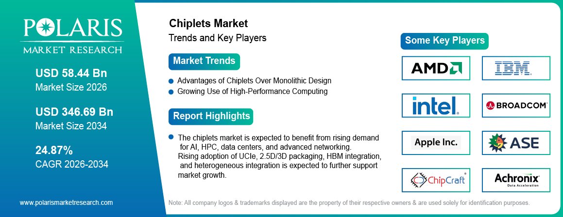
The growth of AI accelerators, custom ASICs, automotive computing, edge computing, silicon photonics, and HBM-based devices is giving rise to new chiplet use cases. As reported by Stanford University, global investments in AI integration exceeded USD 581.7 billion in 2025, rising by 129.9% compared to the previous year. Standards such as UCIe will make it possible to enlarge the market by allowing different vendor chiplets to operate in the same architecture. Improvements in terms of interoperability, testing, 3D packaging, and die-to-die connectivity will contribute to greater commercial success (Source: hai.stanford.edu).
Segmentation Analysis
Chiplets market segmentation includes processor, packaging technology, industry vertical, and region.
By Processor Analysis
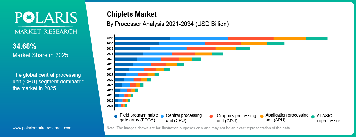
The market is segmented into field programmable gate array (FPGA), graphics processing unit (GPU), central processing unit (CPU), application processing unit (APU), and AI-ASIC coprocessor. The Central Processing Unit (CPU) segment dominated with 34.68% revenue share in 2025. CPU is an essential processor for many computing devices. CPU manufacturers' increasing focus on energy efficiency, scalability, and higher processing power will significantly contribute to this segment growth. Moreover, the ability of chiplets to increase efficiency and organize CPU design allows CPU manufacturers to concentrate on the adoption of this technology. Thus, with the increasing need of CPU in a wide range of applications from consumer electronics to data centers, the demand for chiplets is expected to increase in the coming years.
The AI-ASIC coprocessor segment is anticipated to expand at a considerable CAGR of 34.68% during the projected period. The growth is driven by the need for AI processing, memory bandwidth, and efficient computing. Chiplets will support the integration of accelerator, memory, I/O, and communication into the same package in the design of the AI-ASIC coprocessors.
By Packaging Technology Analysis
The 2.5D/3D segment held the dominant share of 37.68% in 2025. The assurance of excellent performance, miniaturization, and bandwidth provided by this packaging technology, owing to the vertical stacking of chiplets, contributes to the segment’s largest share. Moreover, this technology makes it possible to include multiple ICs in the same package. Thus, the benefits of high package density and energy efficiency have made 2.5D/3D technology an ideal chiplet integration platform. Improvements in technologies such as TSMC’s CoWoS and SoIC, Intel’s Foveros, and other 3D integration approaches are further aiding adoption. The growing adoption of 2.5D/3D packaging is also driving demand for advanced IC substrates, which provide the fine-line routing and high layer counts needed to connect multiple chiplets within a single package.
| Attribute | Best Suited For | Key Advantage |
| 2.5D/3D | CPUs, mobile APs, AI accelerators, display driver ICs | Highest die-to-die interconnect density and vertical stacking |
| System-in-Package (SiP) | Consumer electronics, automotive, healthcare, industrial IoT | Flexible integration of heterogeneous components |
| Flip Chip Chip Scale Package (FCCSP) | High-performance mobile devices, 5G, automotive ADAS | Low inductance, higher routing density for high-frequency signals |
| Flip Chip Ball Grid Array (FCBGA) | High-performance processors, data center applications | Superior thermal dissipation and electrical performance |
| Wafer-Level Chip Scale Package (WLCSP) | Space-constrained consumer devices | Shorter interconnects, cost-effectiveness |
| Fan-Out (FO) | RF components, sensor integration | Simplified integration without a substrate |
Source: Polaris Market Research Analysis
By Industry Vertical Analysis
The consumer electronics segment generated the significant revenue share of 27.68% in 2025. Increasing demand for thinner and lighter designs of portable laptops and ultrabooks owing to the use of chiplet technology fueled the segmental growth. Moreover, factors such as rising use of chiplets for viewing higher quality video-content on smart TVs and the rapid growth of consumer electronics sector would fuel the segmental growth during the forecast period. According to the Ministry of Industry and Information Technology, China’s electronic information manufacturing output grew 10.6% year over year in January to October 2025, while integrated circuit production rose 10.2% to 386.6 billion units (Source: gov.cn).
The automotive segment is expected to register the highest CAGR of 26.91% during the forecast period. This is due to the increasing use of ADAS, self-driving cars, software defined cars, and high-performance vehicle computing. Automotive chiplets allow automotive manufacturers to include processing power, AI acceleration, connectivity, and other features in compact systems.
Applications of Chiplets in AI and High-Performance Computing
AI and HPC are the important use cases for chiplets. They require very high performance computing, high memory bandwidths, and computing specialization capabilities. Chiplets architecture makes it possible to incorporate CPU cores, AI accelerators, I/O dies, networking, and HBM into one package.
Increasing investments in AI infrastructure boost the adoption of chiplets. Some companies like Intel, AMD, TSMC, Samsung, and ASE are providing their advanced packaging technologies and chiplets suitable for AI and HPC applications. This solution is also useful because it enables combining special dies without creating a huge monolithic chip.
Chiplets in Data Centers and 5G Networks
There is a rising need for chiplets in data centers due to the increasing use of AI accelerators, custom ASICs, CPUs, networking processors, and HBM technology. The design of chiplets allows combining specific features while keeping performance, power consumption, scalability, and production costs balanced.
5G networks provide growth potential through the integration of networking processors, RF systems, accelerators, and edge computing platforms. Advanced chiplet packaging technologies will enable greater bandwidth and compact designs, and the adoption of 5G chipsets increases the overall scope of opportunity.
Open Chiplet Ecosystem & UCIe Standard
UCIe chiplet standard is contributing to an open chiplet ecosystem through its provision of a standardized architecture that enables die-to-die communications. The features incorporated in UCIe 2.0 include management, testing, debugging, and 3D packaging, while those introduced in UCIe 3.0 include increased data rates and capabilities for high-performance chiplets.
With the rising popularity of UCIe, multi-vendor chiplet integration will be boosted by providing an opportunity to integrate dies from different manufacturers into common architectures. It will allow avoiding the obligation to design each part independently and provide more flexibility in the applications of AI, HPC, automotive, networking, and many others.
Regional Snapshot
| Region | Key Market Factors | Market Outlook |
| Asia Pacific | Strong semiconductor manufacturing, foundry, OSAT, and advanced packaging ecosystem | Major market |
| North America | AI, HPC, data centers, advanced processors, and semiconductor innovation | High growth potential |
| Europe | Automotive electronics, industrial automation, and semiconductor R&D | Emerging market |
| Latin America | Electronics, telecommunications, industrial automation, and data center investment | Developing market |
| Middle East & Africa | AI adoption, digitalization, data centers, and advanced computing infrastructure | Emerging market |
Source: Polaris Market Research Analysis
Asia Pacific
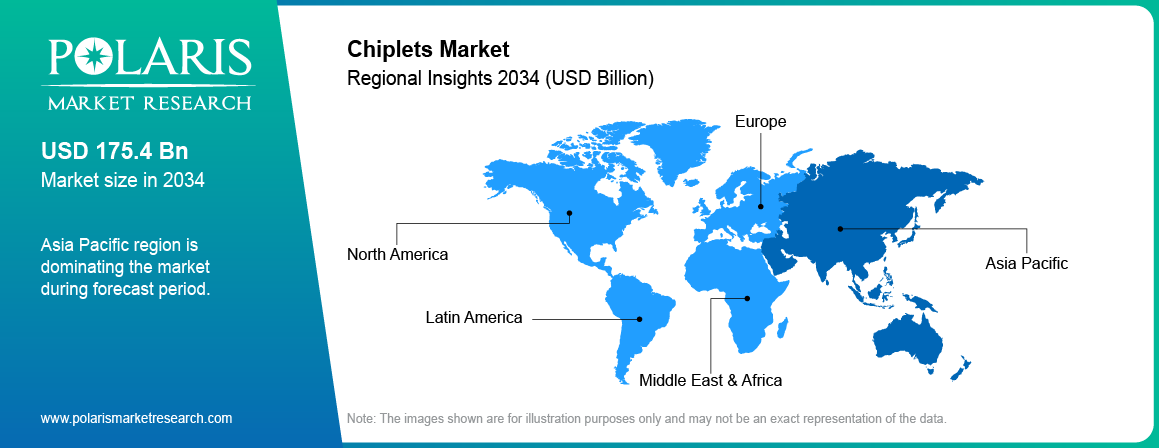
Asia Pacific dominated the global chiplets market in 2025 and is projected to register the highest CAGR of 25.86% during the forecast period. The dominance of this region is attributed to the factors such as investments in research & development, supportive regulatory framework, government-led programs for digital transformation, and expansion of the consumer electronics industry. Moreover, the chiplets market growth is driven by the expanded Asia Pacific semiconductor industry, which is home to a strong network of manufacturers, technology innovators, and foundries.
An increasing demand for electronic devices from the highly populous countries such as China and India will fuel the growth of Asia Pacific chiplets market during the forecast period. Moreover, increasing government support for the research & development of this technology is expected to fuel the market growth. In September 2026, Synopsys and Singapore’s A*STAR signed an MoU to advance simulation-led semiconductor packaging and chiplet technologies for AI and high-performance computing (Source: eetasia.com).
North America
The North America chiplet market is expected to record a significant CAGR of 26.67% during the forecast period. This is due to its leadership in processor design, AI accelerators, data centers, and semiconductor IP. Rigetti received USD 100 million from the CHIPS Act by the U.S. government in September 2026 to support R&D of scalable superconducting quantum computing. Some major companies in the U.S. include Intel, AMD, NVIDIA, Apple, and Marvell. In addition, the growing domestic investments in semiconductors and advanced packaging is driving regional development (Source: rigetti.com).
Europe
The Europe chiplets Market is expected to register a CAGR of 23.41% during the projected period. This is due to its automotive, industrial automation, semiconductor manufacturing equipment, and research ecosystems. According to ACEA, there was a 2.4% increase in EU, UK, and European Free Trade Association automobile sales in November 2025, with EU sales increasing by 2.1% to 900,000 units. The number of registrations of battery electric, hybrid, and plug-in hybrid vehicles in 2025 was up 44.1%, 38.4%, and 4.2%, respectively, thus making their combined share of EU registration of 65.6%. The demand for ADAS, autonomous driving, and software-defined vehicles will create market opportunities for automotive computing chiplets (Source: reuters.com).
Latin America
The Latin America chiplet market is expected to register a CAGR of 22.76% during the projected period. Its expansion is attributed to growing demand for electronics, industrial automation, telecommunications, and data center infrastructure. However, its adoption is expected to be gradual due to smaller semiconductor manufacturing and advanced packaging ecosystem in the region.
Middle East & Africa
The Middle East & Africa chiplet market is projected to exhibit a CAGR of 21.93% during the forecast period,. Its growth is supported by digital transformation, growth in data centers, telecommunication, and investments in high-performance computing infrastructure. Increased use of AI and digitization of industries has generated opportunities for the use of chiplets in the region despite its dependence on semiconductor supply chains across the globe.
Technological Advancements in Chiplets
Some of the technological advancements that could impact the next wave of chiplets include:
-
Hybrid bonding: Shorter interconnects and denser die-to-die interconnects
-
Larger 2.5D packages: More compute dies and HBM stacks can be supported.
-
Panel-level packaging: Potential for better material efficiency and scalability.
-
Glass interposers: Lower signal loss and larger package sizes for 2.5D integration.
-
Interconnects based on UCIe: Enables interoperability among chiplets
-
Integration of HBM: Enabling high-bandwidth AI/HPC computing.
-
Silicon Photonics: Enabling high-speed optical communications.
-
AI-specific chiplets: Enables dedicated accelerators and generic computing chips to be combined.
-
Thermal Management: Gains more relevance with higher packaging density.
TSMC is working towards building a more substantial CoWoS solution for HPC and HBM needs, while ASE is working on panel level packaging to counter the increasing complexities of AI chips.
Security Challenges in Chiplet Architectures
Security becomes an issue with chiplet architecture because different dies, IP cores, vendors, and interfaces can all be integrated into one solution.
Key risks include:
- Unauthorized modification of chiplet IP.
- Counterfeit or compromised chiplets.
- Vulnerabilities in die-to-die interfaces.
- Side-channel and hardware attacks.
- Supply-chain security concerns.
- Difficulty validating third-party chiplets.
- Security gaps across multi-vendor ecosystems.
Therefore, chiplet security needs to be considered throughout chiplet design, manufacturing, testing, packaging, and system deployment.
Open standards such as UCIe are increasingly adding manageability, testing, debug, and lifecycle capabilities that can support stronger system-level validation.
Competitive Insights
The semiconductor chiplets market includes semiconductor designers, foundries, advanced packaging companies, OSAT providers, interconnect technology companies, and semiconductor IP suppliers. Competition is increasingly shifting beyond processor performance toward advanced packaging capacity, chiplet interoperability, die-to-die connectivity, HBM integration, thermal management, and ecosystem partnerships. Chiplet companies focus on chiplet technological advancements. The companies are concentrating on improving their market shares. They adopt various strategies such as mergers and acquisitions and new product launches with chiplet technologies.
List of Chiplet Market Key Players
- Achronix Semiconductor Corporation
- Advanced Micro Devices, Inc. (AMD)
- Apple Inc.
- ASE Technology Holding Co., Ltd.
- Broadcom Inc.
- ChipCraft
- IBM
- Intel Corporation
- Marvell Technology
- MediaTek
- NVIDIA Corporation
- Qualcomm Incorporated
- Ranovus
- Samsung Electronics Co., Ltd.
- Taiwan Semiconductor Manufacturing Company Limited (TSMC)
- YorChip
Competitive Benchmarking
| Company | HQ | Chiplet Focus Area |
| Intel Corporation | U.S. | Foveros / EMIB packaging; CPU and AI accelerator chips |
| Advanced Micro Devices, Inc. (AMD) | U.S. | Infinity Fabric interconnect; Ryzen/EPYC modular CPU and GPU chiplets |
| Apple Inc. | U.S. | Custom silicon chiplet integration for consumer devices |
| IBM | U.S. | Chiplet packaging partnership with Rapidus for next-gen 2nm devices |
| Marvell Technology | U.S. | High-speed silicon interconnects for data center chiplets |
| MediaTek | Taiwan | 2nm chiplet-inspired ASIC design for AI acceleration |
| NVIDIA Corporation | U.S. | GPU chiplet strategy and HPC system acquisitions |
| ASE Technology Holding | Taiwan | Advanced packaging and test services for chiplet assembly |
Source: Polaris Market Research Analysis
Recent Developments
- in September 2026, Arteris expanded its multi-die portfolio with FlexGen Multi-Die. It enables efficient data movement across chiplets as the industry shifts from monolithic SoCs to chiplet-based architectures. (Source: finance.yahoo.com)
- In September 2026, EdgeCortix signed a multi-year, multimillion-dollar agreement with Kawasaki Heavy Industries to develop AI-enabled aerial defense systems using chiplet-based edge AI technologies. (Source: businesswire.com)
- In July 2026, Eliyan introduced NuLink-XD, a 224G PAM4 SerDes architecture designed on TSMC’s 3nm process to enable up to 40% lower power consumption for AI and chiplet-based interconnects. (Source: eliyan.com)
- In July 2026, TYLsemi raised USD 43 million to launch a full-stack chiplet platform for custom AI silicon, spanning connectivity, power delivery, and memory. (Source: semiconductor-digest.com)
- In May 2026, AMD announced over USD 10 billion in Taiwan investments to advance chiplet-based architectures and advanced packaging for AI infrastructure. (Source: amd.com)
Future Outlook
The chiplets market is expected to benefit from rising demand for AI, HPC, data centers, and advanced networking. Rising adoption of UCIe, 2.5D/3D packaging, HBM integration, and heterogeneous integration is expected to further support market growth. Interoperability, packaging capability, cost-effectiveness, thermal management, and testing will probably characterize future competition. Those organizations that have strong capabilities in chiplet design, advanced packaging, interconnect, and system integration are expected to have competitive edge over others.
Research Methodology
Chiplets Market Analysis is done using both the Top-down and Bottom-up approach, backed by Data Triangulation. Secondary Research includes information from the reports, industry magazines, technological advancements, patents, launches, and announcements made by the players in the industry.
Primary research includes discussion with the semiconductor designers, foundries, OSATs, packagers, equipment manufacturers, and end-users for the validation of processor mix, packaging usage, regional demand, and technology trends.
Market revenues are estimated across processor, packaging technology, industry vertical, and regional segments and cross-checked against the broader semiconductor and advanced packaging markets. The existing Polaris forecast also requires analyst re-verification due to significant differences between current industry estimates and the published market figures.
Chiplets Market Segmentation
By Processor Outlook (Revenue, USD Billion, 2021–2034)
- Field Programmable Gate Array (FPGA)
- Graphics Processing Unit (GPU)
- Central Processing Unit (CPU)
- Application Processing Unit (APU)
- AI-ASIC Coprocessor
By Packaging Technology Outlook (Revenue, USD Billion, 2021–2034)
- System-in-Package (SiP)
- Flip-Chip Chip Scale Package (FCCSP)
- Flip Chip Ball Grid Array (FCBGA)
- 2.5D/3D
- Wafer Level Chip Scale Package (WLCSP)
- Fan-Out (FO)
By Industry Vertical Outlook (Revenue, USD Billion, 2021–2034)
- Enterprise Electronics
- Consumer Electronics
- Automotive
- Industrial Automation
- Healthcare
- Military & Aerospace
- Others
By Regional Outlook (Revenue, USD Billion, 2021–2034)
- North America
- U.S.
- Canada
- Europe
- Germany
- France
- UK
- Italy
- Spain
- Netherlands
- Russia
- Rest of Europe
- Asia Pacific
- China
- Japan
- India
- Malaysia
- South Korea
- Indonesia
- Australia
- Vietnam
- Rest of Asia Pacific
- Middle East & Africa
- Saudi Arabia
- UAE
- Israel
- South Africa
- Rest of Middle East & Africa
- Latin America
- Mexico
- Brazil
- Argentina
- Rest of Latin America
Chiplets Market Report Scope
| Report Attributes | Details |
| Market Size in 2025 | USD 46.98 Billion |
| Market Size in 2026 | USD 58.44 Billion |
| Revenue Forecast by 2034 | USD 346.69 Billion |
| CAGR | 24.87% from 2026 to 2034 |
| Base Year | 2025 |
| Historical Data | 2021–2024 |
| Forecast Period | 2026–2034 |
| Quantitative Units | Revenue in USD Billion and CAGR from 2026 to 2034 |
| Report Coverage | Revenue Forecast, Competitive Landscape, Growth Factors, and Industry Trends |
| Segments Covered |
|
| Regional Scope |
|
| Competitive Landscape |
|
| Report Format |
|
| Customization | Report customization as per your requirements with respect to countries, regions, and segmentation. |
Source: Polaris Market Research Analysis
Report Coverage
The chiplets market report provides a detailed assessment of market size, growth trends, competitive developments, processor types, packaging technologies, industry verticals, and regional markets. The study examines the growing adoption of chiplet architectures across CPUs, GPUs, AI accelerators, enterprise electronics, consumer electronics, automotive systems, industrial applications, healthcare, and aerospace & defense. The report also evaluates advanced packaging technologies, AI and HPC applications, data center adoption, UCIe development, competitive strategies, technological advancements, market opportunities, and key industry developments.
Chiplets Market FAQ's
Chiplets are the customized semiconductor die that are combined in one package to perform functions like computing, memory, I/O, or AI acceleration.
The market was valued at USD 46.98 billion in 2025 and is expected to grow to USD 346.69 billion in 2034, at a CAGR of 24.87%.
Some of the factors influencing the growth of the market include AI, HPC, data centers, advanced packaging, HBM, and need for scalability in semiconductor architecture.
The CPU segment holds prominence with rising usage of chiplets in servers, PC, data centers, and computing platforms.
The 2.5D/3D packaging segment dominates the market owing to its density, bandwidth, and usage in AI and HPC applications.
Enterprise electronics industry presents huge potential owing to increasing demand for AI infrastructure, data centers, servers, and interconnections.
The UCIe standard is the open die-to-die interconnect technology that helps in making chiplets compatible and provides support to multi-die architecture scalability.
Some of the major challenges include testing, cost of packaging, heat dissipation, interconnect reliability, compatibility, security, and supply chain management.
Asia Pacific lead the market owing to its robust semiconductor fabrication, packaging, and electronics industry base.
Download Sample Report of Chiplets Market
Please fill out the form to request a customized copy of the research report.


