
U.S. Semiconductor Defect Inspection Equipment Market Share & Trend Report 2026-2034
REPORT DETAILS
REPORT DETAILS
ABOUT THIS REPORT
U.S. Semiconductor Defect Inspection Equipment Market Summary
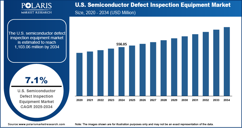
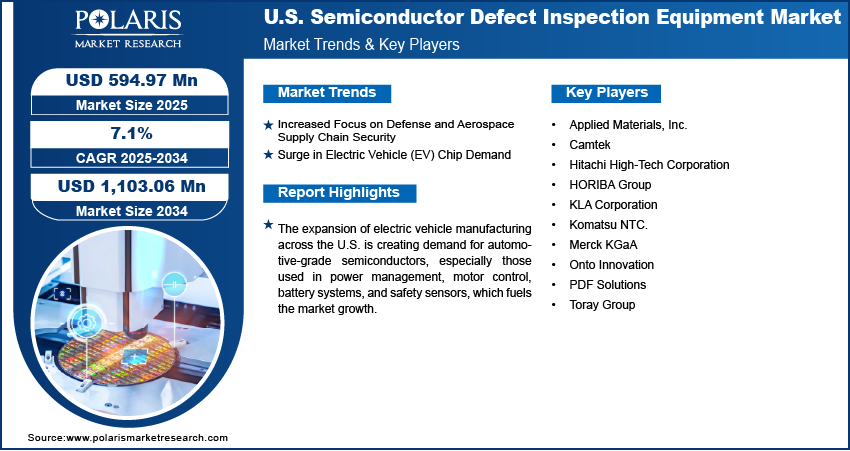
The U.S. semiconductor defect inspection equipment market size was valued at USD 594.97 million in 2025, growing at a CAGR of 7.1% from 2026 to 2034. Government incentives through the CHIPS and Science Act are propelling the expansion of semiconductor manufacturing in the U.S., leading to increased installation of defect inspection tools
Market Statistics
Key Takeaways
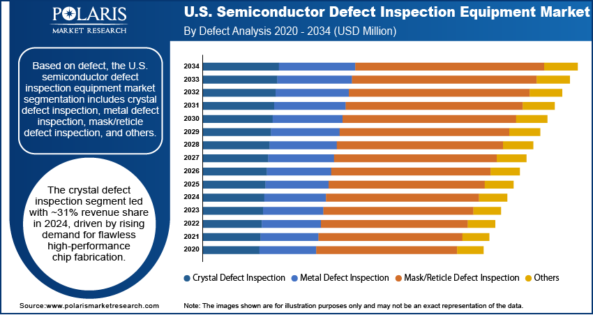
- The crystal defect inspection segment dominated the market in 2025 with 31.4% of the revenue share due to increased production of high-performance chips.
- The machine learning and AI segment is expected to register the highest CAGR of 10.1% from 2026 to 2034, as rising chip complexity and data-intensive inspection environments are accelerating the adoption of machine learning and AI algorithms in defect inspection systems.
Note: Figures and projections outlined in this report are the result of Polaris Market Research’s proprietary analytical processes, grounded in the latest available datasets and market observations.
Industry Dynamics
- Rising demand for high-performance chips in AI, automotive, and data centers is driving investments in advanced defect inspection technologies.
- Increasing complexity of semiconductor nodes requires more precise and frequent defect detection during manufacturing processes.
- Opportunity exists in integrating AI and machine learning into inspection systems for faster, more accurate defect classification and predictive maintenance.
- High equipment costs and limited availability of skilled technicians hinder widespread adoption in smaller semiconductor facilities.
AI Artificial intelligence facilitates high-precision defect detection at nanometer-scale nodes.
- Machine learning (ML) is used to improve defect classification accuracy. It helps reduce false positives.
- AI-enabled systems support real-time inspection during wafer processing.
- Integration of the technology enhances yield management and process optimization.
- It reduces reliance on manual inspection. This improves throughput and productivity.
Source: Polaris Market Research Analysis
What is Semiconductor Defect Inspection Equipment?
Semiconductor defect inspection equipment refers to advanced systems used in chip manufacturing. The equipment is used to detect, classify, and analyze defects across wafers, photomasks, and packaging stages. These tools leverage optical, e-beam, and AI-driven technologies. They help ensure precise process control, maximize yield, and maintain reliability in increasingly complex semiconductor production environments
The U.S. semiconductor defect inspection equipment market focuses on tools and systems used to detect, classify, and analyze defects in semiconductor wafers, photomasks, and packaging. These systems ensure yield optimization, process control, and quality assurance during semiconductor manufacturing, supporting both front-end and back-end production. The U.S.-based fabs are accelerating production at advanced nodes such as 5nm and 3nm. These smaller geometries make semiconductor structures more vulnerable to micro-defects, necessitating the deployment of advanced inspection machines to maintain process control and ensure device performance in high-density chips.
The growing demand for AI accelerators and high-performance computing chips is increasing complexity in semiconductor design and production. Inspection systems play a crucial role in ensuring wafer quality at every layer, thereby supporting the error-free fabrication of processors used in data centers, research, and edge computing. Moreover, major foundry expansions are underway in the U.S., including greenfield fabs focused on logic, memory, and analog devices. Each phase of construction involves large-scale installation of metrology and defect detection systems to ensure cleanroom integrity and maintain competitive yield levels.
Comparison Between Optical vs E-Beam Inspection Systems
Semiconductor defect inspection relies on two primary technologies: optical and e-beam systems. Each system serves distinct roles in the manufacturing process. Optical inspection is used for high-speed, large-scale monitoring. However, e-beam inspection provides ultra-high resolution for advanced node analysis. They form a complementary approach to ensure accuracy, yield optimization, and process control.
| Aspect | Optical Inspection Systems | E-Beam Inspection Systems |
| Technology | Uses light (laser/UV) and imaging sensors | Uses focused electron beams for scanning |
| Resolution | Moderate; limited at advanced nodes | Ultra-high; suitable for sub-10 nm defects |
| Speed | Very high throughput; ideal for inline inspection | Slower; used for detailed analysis |
| Defect Detection | Best for surface and pattern defects | Detects buried, subtle, and nanoscale defects |
| Application Stage | Frontline monitoring in high-volume manufacturing | Failure analysis and critical defect review |
| Cost | Lower cost per inspection | Higher equipment and operating cost |
| Data Output | 2D imaging with pattern comparison | High-resolution 2D/3D-like detailed imaging |
| Use Case | Routine wafer and mask inspection | Advanced node inspection and R&D |
Source: Polaris Market Research Analysis
Drivers and Opportunities
Increased Focus on Defense and Aerospace Supply Chain Security: Growing concerns over national security and technological sovereignty have led to a renewed emphasis on strengthening the domestic semiconductor supply chain for defense and aerospace applications. According to the Aerospace Industries Association, in 2023, the U.S. aerospace and defense sales exceeded USD 955 billion, marking a 7.1% growth from the previous year. Critical systems used in satellites, avionics, radar, and missile guidance demand flawless, high-reliability semiconductor components that perform consistently under extreme conditions. This demand has triggered a significant shift in manufacturing strategy, prompting U.S.-based defense contractors and chipmakers to invest in secure, in-house fabrication capabilities.
Surge in Electric Vehicle (EV) Chip Demand: The expansion of electric vehicle manufacturing across the U.S. is creating demand for automotive-grade semiconductors, especially those used in power management, motor control, battery systems, and safety sensors. According to the U.S. Energy Information Administration, Tesla’s market share accounted for 48.9% of the total electric vehicle market in 2Q24. These chips must meet stringent standards related to thermal stability, durability, and failure tolerance under variable road and climate conditions. Given the safety-critical nature of these components, defect inspection equipment has become indispensable to EV chip production workflows.
Source: Polaris Market Research Analysis
Segmental Insights
Defect Analysis
Based on defect, the U.S. semiconductor defect inspection equipment market segmentation includes crystal defect inspection, metal defect inspection, mask/reticle defect inspection, and others. The crystal defect inspection segment dominated the market in 2025 with 31.4% of the revenue share as the increased production of high-performance chips has elevated the need to detect even the slightest imperfections in crystal structures during wafer fabrication. These defects, such as dislocations or stacking faults, severely impact transistor behavior, reliability, and device yield, especially at smaller nodes. Leading-edge fabs operating at sub-7nm scales rely on advanced optical and X-ray-based tools to identify abnormalities in the crystal lattice that results from thermal stress, process variations, or material inconsistencies.
Inspection Technique Analysis
In terms of inspection technique, the U.S. semiconductor defect inspection equipment market segmentation includes 2D inspection techniques, 3D inspection techniques, and machine learning and AI. The machine learning and AI segment is expected to register the highest CAGR of 10.1% from 2026 to 2034, as rising chip complexity and data-intensive inspection environments boost the adoption of machine learning and AI algorithms in defect inspection systems. These technologies enhance pattern recognition, classify anomalies in real time, and adapt to evolving defect types that traditional rule-based systems may overlook. As fabs transition to advanced nodes and heterogeneous integration, inspection workloads become more demanding, requiring intelligent systems that differentiate between nuisance defects and yield-critical issues with greater accuracy. AI-based tools reduce false positives, optimize process control, and improve decision-making across the production line.
Source: Polaris Market Research Analysis
Key Players and Competitive Analysis Report
The competitive landscape of the U.S. semiconductor defect inspection equipment market is shaped by rapid innovation cycles, strategic technology alliances, and an increasing focus on advanced node capability. Companies are aggressively pursuing market expansion strategies that include investments in R&D to develop high-resolution, AI-integrated inspection platforms capable of detecting sub-nanometer defects. Mergers and acquisitions are playing a central role in consolidating niche capabilities such as e-beam inspection and deep learning analytics, followed by post-merger integration to streamline product portfolios. Strategic alliances between inspection system providers and chip manufacturers are emerging to co-develop customized inspection solutions tailored for EUV lithography and advanced packaging.
A few major companies operating in the U.S. semiconductor defect inspection equipment market include Applied Materials, Inc.; Camtek; Hitachi High-Tech Corporation; HORIBA Group; KLA Corporation; Komatsu NTC.; Merck KGaA; Onto Innovation; PDF Solutions; and Toray Group.
Key Players
- Applied Materials, Inc.
- Camtek
- Hitachi High-Tech Corporation
- HORIBA Group
- KLA Corporation
- Komatsu NTC.
- Merck KGaA
- Onto Innovation
- PDF Solutions
- Toray Group
U.S. Semiconductor Defect Inspection Equipment Industry Developments
In February 2025, TORAY ENGINEERING Co., Ltd. launched a novel inspection system for large glass substrates in the advanced semiconductor packaging industry, featuring double-sided inspection and internal defect detection. (Source: toray-eng.com)
In October 2024, Merck acquired Unity-SC, a company specializing in metrology and inspection instrumentation. This acquisition enhances Merck's capabilities in critical technologies relevant to artificial intelligence applications, particularly in the area of Heterogeneous Integration. (Source: merckgroup.com)
What is the Future of the U.S. Semiconductor Defect Inspection Equipment market?
The market is poised for strong growth in the coming years. It would be driven by rising demand for AI chips and advanced node manufacturing. Increasing semiconductor consumption across industries will also boost the growth. Also, ongoing fab expansions are accelerating equipment adoption. Continuous innovation in inspection technologies, including AI integration and high-resolution systems, will enhance precision. It will enable improved yield optimization and process efficiency.
U.S. Semiconductor Defect Inspection Equipment Market Segmentation
By Defect Outlook (Revenue, USD Million, 2021–2034)
- Crystal Defect Inspection
- Metal Defect Inspection
- Mask/Reticle Defect Inspection
- Others
By Technology Outlook (Revenue, USD Million, 2021–2034)
- Optical Inspection
- Electron Beam Inspection
- X-ray Inspection
- Others
By Inspection Technique Outlook (Revenue, USD Million, 2021–2034)
- 2D Inspection Techniques
- 3D Inspection Techniques
- Machine Learning and AI
By Process Stage Outlook (Revenue, USD Million, 2021–2034)
- Front-End of Line (FEOL)
- Back-End of Line (BEOL)
- Photomask Shops / Reticle Inspection
- Packaging & Assembly
- R&D and Failure Analysis
By End Use Outlook (Revenue, USD Million, 2021–2034)
- Foundry
- Memory
- Logic
- Integrated Device Manufacturer (IDM)
U.S. Semiconductor Defect Inspection Equipment Market Report Scope
| Report Attributes | Details |
| Market Size in 2025 | USD 594.97 million |
| Market Size in 2026 | USD 645.21 million |
| Revenue Forecast by 2034 | USD 1,103.06 million |
| CAGR | 7.1% from 2026 to 2034 |
| Base Year | 2025 |
| Historical Data | 2021–2024 |
| Forecast Period | 2026–2034 |
| Quantitative Units | Revenue in USD million and CAGR from 2026 to 2034 |
| Report Coverage | Revenue Forecast, Competitive Landscape, Growth Factors, and Industry Trends |
| Segments Covered |
|
| Competitive Landscape |
|
| Report Format |
|
| Customization | Report customization as per your requirements with respect to countries, regions, and segmentation. |
FAQ's
The market size was valued at USD 594.97 million in 2025 and is projected to grow to USD 1,103.06 million by 2034.
The market is projected to register a CAGR of 7.1% during the forecast period.
A few of the key players in the market are Applied Materials, Inc.; Camtek; Hitachi High-Tech Corporation; HORIBA Group; KLA Corporation; Komatsu NTC.; Merck KGaA; Onto Innovation; PDF Solutions; and Toray Group.
The crystal defect inspection segment dominated the market with 31.4% of the revenue share in 2025, as the increased production of high-performance chips has elevated the need to detect even the slightest imperfections in crystal structures during wafer fabrication.
The machine learning and AI segment is expected to register the highest CAGR of 10.1% from 2026 to 2034, fueled by rising chip complexity and data-intensive inspection environments are accelerating the adoption of machine learning and AI algorithms in defect inspection systems.
Download Sample Report of U.S. Semiconductor Defect Inspection Equipment Market
Please fill out the form to request a customized copy of the research report.
