
Glass Substrate Market Size, Share, Trends & Forecast, 2026–2034
REPORT DETAILS
Glass Substrate Market Summary
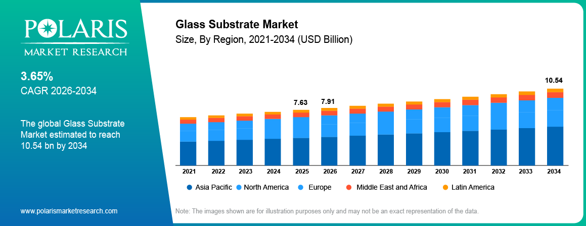
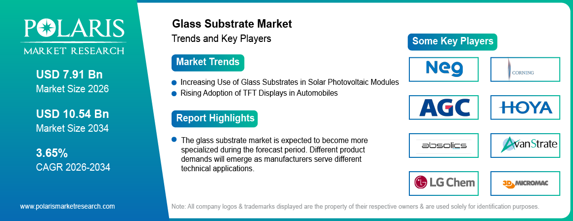
The global glass substrate market size was valued at USD 7.63 billion in 2025. The market is projected to account for a CAGR of 3.65% from 2026 to 2034. Increased usage of glass substrate in solar photovoltaic modules is one of the key factors driving the glass substrate market growth. Rising adoption of TFT glass substrates in automobiles is also shaping the market landscape.
Market Statistics
Key Takeaways
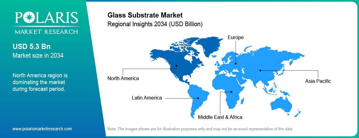
- Asia Pacific accounted for an 52.0% glass substrate market share in 2025. The increased demand for glass substrates from the electronics sector across emerging economies contributes to its major market share.
- North America is projected to grow at an 3.00% CAGR. Technological advancements and rising demand for high-quality panels drive the regional market growth.
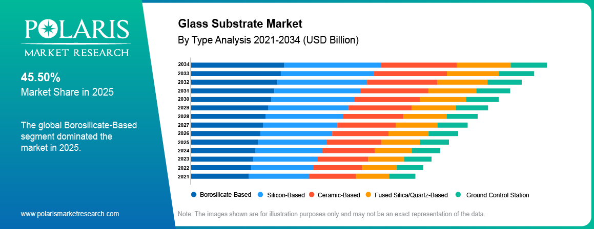
- By type, the borosilicate-based segment held an 45.50% share in 2025. The superior properties of borosilicate contribute to its extensive usage in glass substrates.
- By application, the displays segment led with an 44.50% glass substrate market share in 2025. The segment’s leading position is attributed to high-volume consumer demand.
- By end-use, the automotive segment is projected to grow at an 3.75% CAGR. This is because modern vehicles integrate more digital displays and connected technologies.
Note: Figures and projections outlined in this report are the result of Polaris Market Research’s proprietary analytical processes, grounded in the latest available datasets and market observations.
What is a Glass Substrate?
A glass substrate refers to flat glass that acts as a base in the manufacturing of various parts. It provides a smooth platform on which further processing is done. Glass substrates are used in display panels, semiconductor packaging, solar panels, among others. Their composition varies based on their use.
How Is Glass Substrate Manufactured?
Mixing of Raw Materials: The first step involves mixing the raw materials such as silica and other materials, which are required to produce a particular type of glass.
Melting: The mixture is then melted and converted into molten glass. Maintaining the temperature plays an important role during the melting process.
Sheet formation: Molten glass is converted into sheet form. It depends upon the type of substrate and the thickness required.
Annealing: The glass sheet is then put under the cooling process to reduce the stresses generated during the sheet formation process.
Cutting and finishing: Glass sheets are then cut into particular sizes. Further finishing processes can also be done depending on the application of the substrate.
Inspection: Quality inspection is done for each substrate for thickness and dimensions, among others.
Market Dynamics
Market Drivers : Increasing Use of Glass Substrates in Solar Photovoltaic Modules
The expansion of solar power generation has led to the increased need for glass substrates used in photovoltaic modules. Glass is needed to protect the cells from external elements and allow light to pass through to the active layer. Increasing sizes and efficiency of the solar modules have increased the demand for high-quality photovoltaic glass. Bifacial modules have also contributed to the rising need for glass, as it can be used on both sides of the module. In addition to that, manufacturers have expanded local production facilities to meet the increasing demand for solar modules. Xinyi Solar ignited its first photovoltaic glass furnace in Indonesia in January 2026. The plant uses ultra-clear rolled photovoltaic glass technology and has a daily melting capacity of 1,200 tonnes. Xinyi Solar stated that the he plant is capable of supplying enough photovoltaic glass to meet the demand for solar modules at a capacity of up to 8 GW per year (source: xinyisolar.com). This highlights the increase in photovoltaic glass manufacturing in Southeast Asia. Thus, increased usage in solar photovoltaic modules is contributing to the glass substrate market development.
Market Drivers : Rising Adoption of TFT Displays in Automobiles
The rise in the adoption of TFT panels for cars is fueling the growth in the glass substrate market. Increasing penetration of digital instrument clusters is being observed in the consumer and commercial segments of the automobile industry. Larger displays are also being integrated by automakers in the infotainment and cockpit systems. TFT displays make use of glass substrates that form the basis of the display panel along with the thin-film transistor. Connected car technologies are also leading to an increased requirement for display technologies in vehicles. Minda Instruments received government permission in August 2026 under the Electronics Components Manufacturing Scheme (ECMS) to produce display module sub-assemblies in India. The company plans to set up a facility for manufacturing the TFT display module sub-assemblies for delivery to its automotive customers (source: business-standard.com). The development represents growth in the production of display modules for automotive use. It contributes to demand for TFT glass substrates used in TFT display systems.
Market Drivers : Growing Demand for Glass Substrates in AI and High-Performance Computing Packaging
The increasing size and complexity of AI processors have attracted greater attention to the use of glass substrates in advanced semiconductor packaging. AI processors are being built using more chiplets and high-bandwidth memory, thus making the size of the packages bigger. There could be warpage and dimensional instability problems with conventional organic substrates when package size becomes larger. Glass has better dimensional stability and can accommodate fine-pitch interconnect structures for large packages. Electrical connectivity through glass can be achieved with through-glass via (TGV). In April 2026, AT&S made announcements about progress in glass core substrate technology for AI and high-performance computing applications. According to the company, its research efforts have shifted to industrial application of this technology, as AI data centers need larger and more complex chip packages (source: ats.net). Thus, these developments signify the emergence of glass substrates into commercial application in advanced packaging. The increasing emphasis on AI and HPC packaging is therefore leading to a new application area for the glass substrate market.
Market Restraints and Challenges : High Manufacturing Costs and Processing Complexity
Production of glass substrates might have relatively high production costs compared to those of established substrates. This is because glass substrates are fragile and need careful handling, especially when cutting, drilling, and treating the surfaces. Any damage will result in fewer usable substrates in each production batch. Production of large and thin substrates might be even more challenging. Through-glass via formation also calls for special equipment. Production of substrates with uniform dimensions and surface quality on larger substrates might be difficult. These may impact the production process and the production costs. Special equipment may be required, which adds to the cost of production. This may act as a hindrance to using glass substrates in applications that rely on established substrates with mature production processes.
Market Opportunities : Growing Demand for Glass Substrates in MicroLED Displays
MicroLED technology is creating a new requirement for high-quality substrates in display production. This technology relies on small-sized LEDs that create pixels in a display screen. Glass acts as a flat substrate when positioning and processing the components. It can also be used in high-precision production due to its dimensional stability. MicroLED technology has been considered for televisions, wearables, monitors, and various display products. This technology has the potential for bright images and longer operating time. As such, it has raised a lot of interest among display manufacturers. Production remains complex, especially when a large number of microscopic LEDs need to be transferred in an accurate manner. Any progress in mass transfer and display production would help in the wider commercialization of this technology. This might raise the demand for specialized glass substrates for microLED production.
Market Opportunities : Increasing Use of Glass in Photonic and Optical Devices
There is also potential for using glass substrates in photonic devices. Such devices operate by sending and processing information via light, rather than electricity. Glass provides some valuable optical properties to those components responsible for light guiding or manipulation. Additionally, it can serve as a solid substrate for creating integrated optical structures along with other components. Photonic devices are under development for optical communication, sensing, imaging, and computing purposes. The increasing demand for fast data transmission contributes to the development of optical technologies. Moreover, improvements in wafer-level manufacturing allow manufacturers to make more consistent photonic components. All these factors may contribute to an expansion of applications for glass substrates in addition to already existing display and solar applications. Glass substrate manufacturers capable of precise fabrication may capitalize on this shift.
Glass Substrate Market Trends : Shift Toward Larger and Thinner Glass Substrates
Glass substrate manufacturers are exploring larger substrates and thinner sheets due to varying demands in displays and semiconductors. The use of larger substrates means that more components could be manufactured in a cycle of production. The use of thinner glass may allow for reduced weight and size of the final product. However, thinner sheets would need extra care in handling. It is becoming increasingly important for substrate manufacturers to improve their forming and finishing operations in order to ensure surface quality over a greater area. The shift is particularly important for substrates used in displays due to the impact of substrate size on the efficiency of manufacturing operations. It is also becoming increasingly important in advanced packaging because of larger package sizes.
Glass Substrate Market Trends : Greater Focus on Low-Defect and High-Precision Glass Surfaces
The production of glass substrates is increasingly focused on surface characteristics and precision in size. Tiny defects may cause problems for the display or hinder further fabrication processes using semiconductors. Thus, manufacturers are now paying more attention to such issues as flatness, thickness uniformity, surface roughness, and particle contamination. The requirements become more demanding as the size of the substrates becomes smaller at the feature level. The advanced packaging industry requires precise via formation and proper alignment in the process. Advances in inspection technology enable companies to find defects early. Automated measurements are now applied for monitoring substrate quality at the increased production scale. The importance of precision is impacting not only the equipment used in manufacturing but also the specifications of the substrates.
Glass Substrates vs. Organic Substrates
Both glass and organic substrates are utilized as base materials for electronic and semiconductor devices. However, the two materials possess different attributes when it comes to their physical properties and processing capability. The former has superior dimensional stability and a more homogeneous surface compared to the latter, which is more flexible and easier to process. The choice between glass substrate vs. organic substrate depends on specific application requirements.
| Parameter | Glass Substrates | Organic Substrates |
| Material | Inorganic glass material | Organic resin-based material |
| Dimensional Stability | High dimensional stability | More prone to dimensional changes |
| Thermal Expansion | Provides controlled thermal expansion | Generally has higher thermal expansion |
| Surface Flatness | High surface flatness and uniformity | Depends on material composition and processing |
| Warpage | Lower warpage at larger dimensions | Greater warpage concerns as dimensions increase |
| Manufacturing Cost | Generally higher due to specialized processing | Generally lower due to mature production methods |
| Processing | Requires specialized cutting, drilling, and finishing | Uses established substrate manufacturing processes |
| Flexibility | Rigid and less flexible | Greater mechanical flexibility |
Source: Polaris Market Research Analysis
Report Segmentation
| Segmentation Axis | Segments |
| By Type | Borosilicate-Based · Silicon-Based · Ceramic-Based · Fused Silica/Quartz-Based · Other Types |
| By Application | Displays · Semiconductor Packaging · Solar Cells / Photovoltaics · Sensors & MEMS · Advanced Packaging · Other Applications |
| By End-Use | Electronics · Automotive · Semiconductor · Solar Energy · Healthcare & Medical · Aerospace & Defense · Other End Uses |
| By Region | North America (U.S., Canada) · Europe (Germany, UK, France, Italy, Spain, Netherlands, Russia, Rest of Europe) · Asia Pacific (China, Japan, India, South Korea, Malaysia, Indonesia, Australia, Rest of Asia Pacific) · Latin America (Brazil, Mexico, Argentina, Rest of Latin America) · Middle East & Africa (Saudi Arabia, UAE, Israel, South Africa, Rest of Middle East & Africa) |
Source: Polaris Market Research Analysis
By Type
The borosilicate-based segment led the glass substrate market with an 45.50% share in 2025. Its strong presence in display, electronics, and semiconductor-related applications contributes to its leading market position. The segment benefits from the existing application of the material in sectors where the material is needed for its stability and thermal performance. It is used by display manufacturers as a substrate material in various display panels. Semiconductor uses for the material also include areas where there is a need for a stable and accurate glass surface in the process. Growth in electronic devices is also leading to the adoption of borosilicate glass substrates in various components. There is already an established supply base for this segment, which allows for availability on a large scale. Further investments in displays and semiconductors can ensure the future relevance of the segment.
The fused-silica/quartz-based segment is projected to grow at an 4.40% CAGR. This segment is growing in significance since manufacturers now need substrates that comply with very precise specifications for use in their unique applications. Its position is supported by the rising demand for higher levels of purity of the material being used in the manufacturing process. Fused silica and quartz substrates also have a well-established presence in some precision manufacturing industries. This segment is particularly relevant wherever there are issues of purity and stability of materials due to the nature of the production process. There is an increased investment in semiconductor manufacturing, which is increasing the demand for specialized substrate materials. Photonics and other technologies that involve precision manufacturing are also expanding the potential customer base.
By Application
The displays segment held the largest market share of 44.50% in 2025. Its dominance is attributed to the large number of display panels being manufactured for consumer and commercial electronic applications. Glass substrates are commonly used as base materials in the manufacturing of display panels. The continued recycling of existing old devices is contributing to the steady production volumes of the panels. The shift towards larger screen sizes is contributing to the need for more substrate material per unit of the display panels. Manufacturers of display panels are increasing their manufacturing capacities in electronics manufacturing centers. The increasing adoption of smartphones, television screens, computer monitors, and car screens is contributing to the market base of the segment. At the same time, new display technology developments such as OLED and flat panel display glass are resulting in increased demand for substrates that have tighter manufacturing specifications.
The semiconductor packaging segment is projected to grow at an 4.05% CAGR. This segment is receiving increased focus due to the growing package size and stringent dimensional control needed with increasing sizes. Traditional packaging materials become harder to process as the size of the package increases. Glass substrates provide a steady foundation for making advanced package configurations. Glass substrates have also been explored in the context of interconnect density and high routing density needs. The increasing use of chiplets poses yet another challenge to packaging materials. There has been growing interest in glass core substrate market technologies from semiconductor manufacturers and packaging companies as well. The use of glass substrate for AI chips is also being explored as AI processors require larger and more complex package designs. Glass interposers are another related application being explored for advanced semiconductor packaging. Glass substrates are moving from experimental to commercial development. With increasingly advanced semiconductor architectures, glass substrates are expected to find greater usage in packaging.
By End-Use
The electronics segment held the largest market share of 36.50% in 2025. This position is strengthened by the extensive application of glass substrates in electronic products and components. Growth in consumer and industrial electronics is sustaining the substantial demand for substrates. Ongoing product introductions require continuous production of electronic goods. Increasing demand for thin and smaller products makes precision in substrate materials manufacturing a requirement. At the same time, higher-performance devices are placing greater requirements on the materials utilized in component manufacturing. The development of new capacities for electronics manufacturing fosters the application of special substrates. Glass continues to be a proven material in several electronics manufacturing processes. These factors are helping the electronics sector maintain its leading position among end-users.
The automotive segment is projected to account for an 3.75% CAGR. Increased production of vehicles is resulting in a rise in the use of specialized materials in automotive component production. The shift towards electric and hybrid vehicles has also led to changes in the material requirements for different vehicle platforms. Such vehicles use more electronics and sensing capabilities compared to traditional vehicles. Glass substrates can be applied to certain components where there is a need for a reliable substrate. Sensors are providing another area of application in automotive systems. There is also a trend towards the use of more functional components in smaller component design in vehicles. This has led to an increase in the need for materials that are capable of meeting tight manufacturing specifications.
Use Cases: Glass Substrates in Real-World Applications
The glass substrates act as the basic material for devices that require a flat and stable surface that is manufactured with precision. Their role varies depending on the design and manufacturing of the products. Some uses are well established, but there are new applications evolving from the development of component miniaturization and precision manufacturing.
| Use Case | Glass Substrate Application |
| Display Cover and Panel Structures | Forms part of the panel structure and provides a uniform surface for display components. |
| Touch-Sensing Surfaces | Used as the base for conductive layers that detect touch input. |
| Microfluidic Chips | Glass forms transparent channels and surfaces used to move and examine small fluid samples. |
| Biosensors | Provides a stable platform for sensing materials used in biological detection. |
| Optical Filters | Serve as the base for thin coatings that control the passage of specific wavelengths. |
| Laboratory-on-Chip Systems | Used in compact devices that combine fluid handling with testing or analysis. |
| Precision Optical Components | Supports optical structures where a flat and consistent surface is required. |
| Specialized Research Equipment | Used as a fabrication base in experimental electronic, optical, and sensing devices. |
Source: Polaris Market Research Analysis
Role in Solar Power Systems
Glass is included in the photovoltaic system in the form of the module structure itself. The optical properties of glass influence the interaction of the sunlight with the surface of the cell. The surface of the glass may have specific texturing or coatings that will control the reflection. Glass is used as a surface on which encapsulation layers surround photovoltaic cells. Its properties can sometimes affect heat transfer within the panel. Glass selection varies according to the type of cell used, the design of the module, and its installation requirements. Several factors are considered in determining which glass should be used, including the thickness, optical properties, and surface treatment. The selection of glass has become quite specific as module designs have diversified.
Regional Insights
Asia Pacific
Asia Pacific accounted for an 52.0% glass substrate market share in 2025. Electronics manufacturing is well-established in the region, especially in countries with display and semiconductor industry infrastructure. China continues to be a significant producer of display panels and electronic components. Japan and South Korea are known for manufacturing advanced materials and displays. India is currently developing its electronics and semiconductor manufacturing industry. Manufacturing of solar modules is yet another area that accounts for the demand for glass substrates in Asia Pacific. There is also a widespread supply chain for glass processing and components manufacturing in the region. Investments in manufacturing plants have created a need for substrates of specific thicknesses and surfaces. Growth in the electronics manufacturing industry and related industries is expected to continue driving demand in Asia Pacific.
North America
North America is projected to grow at an 3.00% CAGR. There is an existing base of semiconductor and electronics manufacturing industries in the region that allows for the use of specialty substrates. The US government is also increasing investments in domestic semiconductor production with the construction of fabrication facilities and advanced packaging plants across the country. Glass substrates are gaining traction in these efforts as they can meet the stringent dimensional specifications of new package designs. The region has an existing display and photovoltaic industry base that adds to the addressable market. Research activities by semiconductor firms and materials providers are further supporting work in glass substrates. Canada contributes through its electronics, photonics, and advanced manufacturing industries. Leading technology firms and research institutes in North America continue to promote the development of precision substrates.
Europe
Europe held an 18.00% glass substrate market share in 2025. There is a developed specialty glass industry in the region, providing experience with making materials for demanding applications. Germany has high expertise in industrial glass and precision engineering; the Netherlands is known for its semiconductor equipment ecosystem. Also, France has made progress in photonics and optics; this could result in producing specialized glass substrates. An additional regional consideration is that there are institutes conducting research on advanced materials and manufacturing processes. The preferences for materials have changed because of increasing sustainability demands in European industries. Manufacturers are paying more attention to resource utilization and product longevity. There is also the advantage that the European market is characterized by the presence of high value-added industrial uses rather than consumer-based mass production. These factors are contributing to the growth of glass substrate applications within the region.
Latin America
The Latin America glass substrate market is projected to grow at an 2.70% CAGR. Latin America is witnessing the development of its manufacturing sector for electronics and other technological products, which offers opportunities for increased consumption of specialized glass materials. Brazil has the largest industrial base in the region and contributes significantly to the manufacturing processes. Mexico also has an existing automobile and electronics assembly industry. The development of solar energy applications is another area with strong potential for glass substrate consumption. Moreover, local demand is driven by the application of glass components in technical and industrial equipment. The development of the market is slower compared to regions where there is large-scale production of substrates. However, the growth of industrial activity and the widespread application of advanced technologies are opening up new spheres of application. These factors support the further development of the glass substrate market in Latin America.
Middle East & Africa
The Middle East & Africa glass substrate market is anticipated to account for an 3.20% CAGR. The region is developing its competencies in electronics, renewable energy, and manufacturing. One of the most active sectors in this regard is solar energy, especially in those countries that have extensive renewable energy initiatives. This leads to greater demand for materials utilized in the fabrication of solar modules. The UAE and Saudi Arabia are also developing technological industrial facilities within their economic diversification strategies. Israel adds a strong base in semiconductor materials and other technologies related to precision engineering. In addition, South Africa has manufacturing and research capabilities that contribute to the regional market. Advanced material production in the region is relatively weak when compared to major manufacturing regions. Thus, the regional market relies heavily on importing substrate materials. Further investments in renewables and technology-driven industries are expected to lead to expanded use of glass substrates in the region.
Competitive Landscape
The glass substrate market includes established glass substrate manufacturers and those that are developing new materials with special characteristics. In this industry, competition is influenced by the quality of the product, substrate thickness, surface uniformity, and manufacturing capabilities. Other investments include developing technologies related to semiconductor packaging, displays, photovoltaics, and precision technologies. Increasing production capability is another area of emphasis because of the need for substrates with increasingly stringent specifications in the end-use industries. Another aspect being looked at in terms of capacity expansion is that of end-use industries that demand substrates with more stringent specifications. Through strategic alliances and technological advancements, capabilities are being enhanced in new domains like glass-core substrates and advanced packaging. The competitive landscape differs for different applications, with some companies concentrating on high-volume production while others catering to niche markets.
Vendor Positioning
| Company | HQ | Best known for |
| 3D-Micromac AG | Chemnitz, Germany | Laser micromachining and precision processing solutions for glass and semiconductor materials |
| Covington, Georgia, U.S. | Glass-core substrates for advanced semiconductor packaging | |
| AGC Inc. | Tokyo, Japan | Specialty glass and glass substrates for displays, electronics, and optical applications |
| AvanStrate Inc. | Tokyo, Japan | TFT LCD glass substrates for display panels |
| Corning Incorporated | Corning, New York, U.S. | Large and thin display glass substrates and specialty glass technologies |
| HOYA Corporation | Tokyo, Japan | High-precision glass substrates for data storage and optical applications |
| IRICO Group New Energy Company Limited | Xi'an, China | Photovoltaic glass and solar energy-related glass products |
| Seoul, South Korea | Advanced materials and electronic materials used in semiconductor and display applications | |
| Nippon Electric Glass Co., Ltd. | Otsu, Shiga, Japan | Specialty glass, electronic-device glass, and flat-panel display glass |
| Nippon Sheet Glass Co., Ltd. (NSG Group) | Tokyo, Japan | Specialty and architectural glass, including high-performance glass products |
| Ohara Inc. | Sagamihara, Kanagawa, Japan | Optical glass and specialty glass materials for precision applications |
| Plan Optik AG | Elsoff, Germany | Glass, quartz, and silicon wafers, including glass-core substrates and TGV products |
| Samsung Electro-Mechanics | Suwon, South Korea | High-density semiconductor package substrates, including FCBGA and FCCSP |
| SCHOTT AG | Mainz, Germany | Specialty glass and glass-ceramic materials for high-precision industrial and technology applications |
| Toppan Inc. | Tokyo, Japan | Advanced package substrates and glass substrates with through-glass vias (TGV) |
| Tunghsu Group Co., Ltd.
| Beijing, China
| Photovoltaic glass and solar energy-related materials |
Source: Polaris Market Research Analysis
Cost and Sustainability Considerations
Sustainability considerations have become increasingly relevant in the glass substrate industry as companies evaluate the usage of resources throughout the entire lifecycle of the product. Glass substrates are recyclable and reusable in appropriate production processes, thus reducing the use of virgin resources. Recycling can also assist in decreasing the volume of the waste created in the process. Energy use continues to play an important role because high temperatures are required for the melting of glass.
The efficient use of material is also a priority in terms of producing glass substrates. Material utilization becomes especially significant when the substrates need to be cut to exact sizes for particular purposes. More efficient material utilization can result in less scrap during the production process. The recyclability of glass becomes important at the end of the product's lifecycle.
Industry Developments
- September 2026: SCHOTT launched its RealView® 2.0 glass wafers with a low weight for next-generation augmented reality waveguides. The company stated that the material has been developed with a combination of high refractive index and lower density, which is available in sample sizes and large quantities for several wafer formats. (source: schott.com)
- August 2026: AGC displayed glass substrates for advanced semiconductor packaging and glass carriers for wafer and panel applications at SEMICON India 2026. Additionally, AGC showcased other materials and technologies relevant to semiconductor processing and recycling. (source: agc.com)
- May 2026: SCHOTT launched its knowledge portal “Semicon next” focused on specialty glass solutions for next-generation semiconductors. This initiative covers developments in the areas of glass core substrates, advanced packaging, and through-glass vias. (source: schott.com)
Future Outlook
The glass substrate market is expected to become more specialized during the forecast period. Different product demands will emerge as manufacturers serve different technical applications. More diverse substrate thicknesses, sizes, and compositions might be offered by suppliers to meet these needs. Consistency in quality will remain essential for the industry, as customers set stricter specifications for ready components. The market may see more partnerships between glass manufacturers and companies that process substrates for specific applications. Such partnerships can facilitate the adaptation of glass materials to production demands without the necessity of developing the complete technology by end users. Sourcing strategies might affect the choice of suppliers as well, because access to special glass materials needs to be ensured. Overall, the market is expected to include a greater variety of both established products and specialized substrates.
Research Methodology
The glass substrate market size and forecast are derived through a combination of top-down and bottom-up estimation approaches, cross-validated through primary and secondary research. Secondary research establishes the initial market framework using company annual reports, investor presentations, industry association data, trade publications, and government/customs trade data (e.g., HS code 7005 glass-product trade flows), building out the value chain from raw-material suppliers through glass producers to end-use OEMs.
Primary research validates and refines these estimates through structured interviews with supply-side executives (C-suite, VPs of technology and innovation, product management) and demand-side stakeholders across electronics, automotive, medical, aerospace & defense, and solar power end-use industries. Interview inputs are weighted by company tier (based on annual revenue) to ensure balanced representation across large multinational glass producers and smaller specialty manufacturers.
Market sizing applies data triangulation. It reconciles top-down estimates (derived from parent and peer market sizing) against bottom-up estimates (built from individual company revenues and production volumes). This helps arrive at final segment-level figures for type, application, end-use industry, and region. Forecast assumptions, growth-rate drivers, and risk factors are documented explicitly for each segment, and all figures are revisited at each publication cycle to reflect current base-year data.
Glass Substrate Market Report Scope
| Report Attributes | Details |
| Market Size Value in 2025 | USD 7.63 billion |
| Market Size Value in 2026 | USD 7.91 billion |
| Glass Substrate Market Forecast 2034 | USD 10.54 billion |
| CAGR | 3.65% from 2026 to 2034 |
| Base Year | 2025 |
| Historical Data | 2021–2024 |
| Forecast Period | 2026–2034 |
| Quantitative Units | Revenue in USD billion and CAGR from 2026 to 2034 |
| Report Coverage | Revenue Forecast, Market Competitive Landscape, Growth Factors, and Industry Trends |
| Segments Covered |
|
| Regional Scope |
|
| Competitive Landscape |
|
| Report Format |
|
| Customization | Report customization as per your requirements with respect to countries, regions, and segmentation. |
Glass Substrate Market FAQ's
The glass substrate market size was valued at USD 7.63 billion in 2025. The market is projected to reach USD 10.54 billion by 2034.
The glass substrate industry is projected to account for a 3.65% CAGR from 2026 to 2034.
Asia Pacific held an 52.00% glass substrate market share in 2025. The presence of a well-established electronics manufacturing sector contributes to the region’s major market share.
The automotive segment is anticipated to account for an 3.75% CAGR. This is due to the integration of more digital displays and connected technologies in modern automobiles.
A few of the key market players include 3D-Micromac AG; Absolics Inc.; AGC Inc.; AvanStrate Inc.; Corning Incorporated; HOYA Corporation; IRICO Group New Energy Company Limited; LG Chem, Ltd.; Nippon Electric Glass Co., Ltd.; Nippon Sheet Glass Co., Ltd. (NSG Group); Ohara Inc.; Plan Optik AG; Samsung Electro-Mechanics; SCHOTT AG; Toppan Inc.; and Tunghsu Group Co., Ltd.
A glass substrate for AI chips is a glass-based material being developed for use in advanced semiconductor packages. It can provide a flat and stable base for larger chip packages. Semiconductor companies are studying its use as chip designs become more complex.
Glass substrates are employed in the manufacturing of display screens and photovoltaics. Glass substrates can also be used in selected cases for semiconductors, optics, sensors, and electronics. Glass substrates are finding new applications as companies develop smaller components.
Download Sample Report of Glass Substrate Market
Please fill out the form to request a customized copy of the research report.


